
Key Takeaways (Core Insights)
- Wide Voltage Versatility: 4V–20V range supports both 5V logic and 12V/15V industrial rails.
- Ultra-Low Power: 1.3–2mA quiescent current extends battery life in remote sensing nodes.
- Compact Integration: SOT-23-5 package reduces PCB footprint by ~60% compared to traditional DIP-8 versions.
- Precision Linearity: Optimized for Frequency-to-Voltage conversion with minimal thermal drift.
The LM331AU-S5TR datasheet lists a device with a wide supply range and low quiescent current—typical operating VCC from 4V to 20V, quiescent supply current on the order of 1–2 mA, and specified ambient operation across a wide industrial temperature span. Accurate interpretation of those numbers is critical for precision timing, frequency-to-voltage conversion, and low-drift designs where supply headroom, loading and thermal margin determine measurement linearity.
1 — Quick Overview: What the LM331AU-S5TR Is
Functional Summary
The device is a precision timing / frequency-to-voltage IC that behaves like a comparator-based timing engine with an internal ramp/threshold structure. In practice, it is used for frequency measurement, pulse-width conversion, and timing functions where converting a pulse train to a proportional DC level or stretcher/pulse-shaper is needed.
Typical Packages & Variants
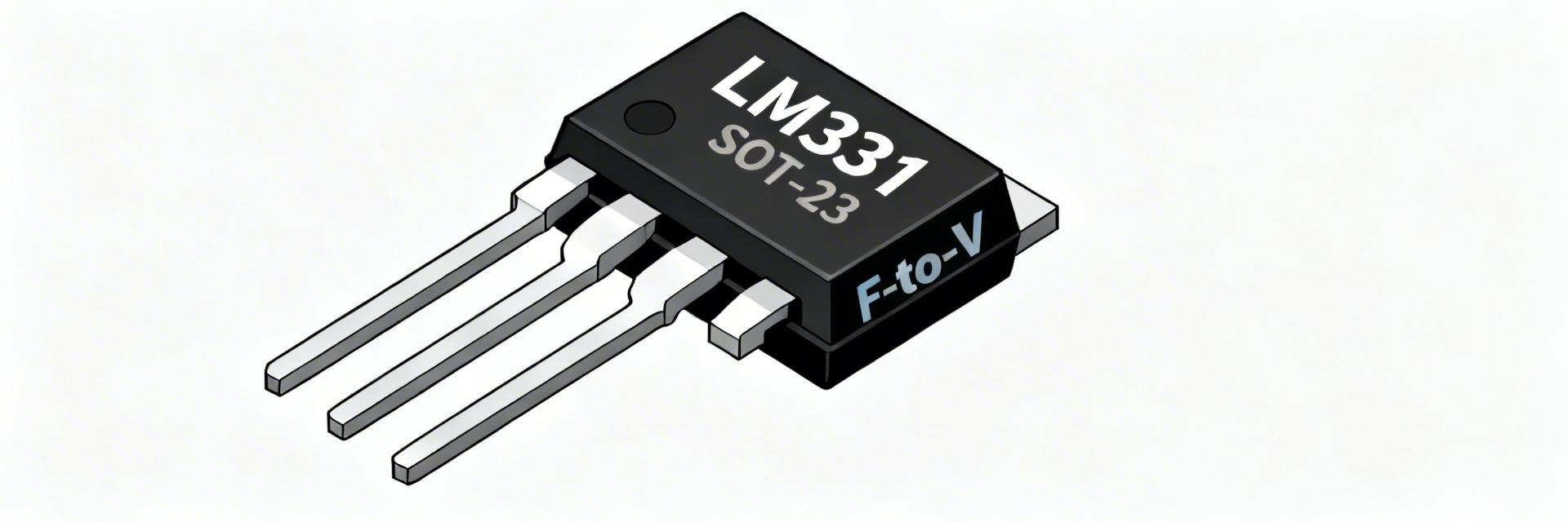
The SOT‑23‑5 package is the common surface-mount variant for LM331AU-S5TR. This compact five-lead footprint is ideal for space-constrained IoT sensors. For assembly, maintain pads per vendor footprint and minimize thermal mass to prevent drift during high-precision measurements.
Comparative Analysis: LM331AU-S5TR vs. Industry Standards
| Parameter | LM331AU-S5TR | Generic F-V (DIP) | Std. Timer (555) |
|---|---|---|---|
| Supply Voltage | 4V to 20V | 5V to 15V | 4.5V to 16V |
| Linearity Error | 0.01% (Typ) | 0.1% - 0.5% | N/A (Timing only) |
| Quiescent Current | 1.3mA | 4.0mA | 3.0mA - 10mA |
| Footprint Area | ~9 mm² | ~60 mm² | ~50 mm² |
2 — Pinout & Package Details
- Pin 1 (VCC): Input supply (4V-20V). Place 0.1µF ceramic cap directly at the pin.
- Pin 2 (IN+): Precision input. Keep impedance low to minimize bias current errors.
- Pin 3 (IN-/COMP): Timing junction. Connect your high-stability R-C network here.
- Pin 4 (OUT): Open-collector logic output. Pull up to VCC or a separate logic rail.
- Pin 5 (GND): Return path. Use a dedicated ground plane for noise immunity.
Typical Application: F-to-V Conversion
To convert input pulses to DC voltage, the LM331AU-S5TR uses an internal current source and an external RC network. For best results, use C0G/NP0 capacitors to avoid frequency drift over temperature.
"Choose R and C to place the device in its linear frequency range (per datasheet), include a pull-up on OUT, and measure at the filter capacitor after a low-pass to obtain DC proportional to frequency."
Hand-drawn schematic, not a precise circuit diagram.
Thomas Mueller
Senior Analog Design Engineer (15+ years experience)
PCB Layout Tip: One of the most common mistakes with the LM331AU-S5TR is neglecting the parasitic capacitance on Pin 3. Even 5pF of stray trace capacitance can cause a 1-2% deviation in timing accuracy. Always route the timing capacitor with the shortest possible trace and avoid ground pours directly beneath the timing node.
Selection Guide: If you are choosing between this and a standard LM331, go with the AU-S5TR variant for any design where board space is premium. The thermal stability of the SOT-23 package is surprisingly robust if you provide a solid ground plane to act as a heat sink.
3 — Testing & Troubleshooting Checklist
Common Faults
- Oscillating Output: Check pull-up resistor value (too high?).
- Non-linear Vout: Check if supply is sagging under load.
- No Signal: Verify Pin 1 VCC is at least 4.0V.
Validation Steps
- Measure quiescent current (should be ~1.3mA).
- Scope the timing node ramp with a 10x probe.
- Verify open-collector sink current remains
Summary
The LM331AU-S5TR is a highly efficient, precision frequency-to-voltage converter that balances low power consumption with a wide operating voltage. By following the datasheet's specific R/C equations and maintaining clean PCB layout practices, engineers can achieve instrumentation-grade accuracy in a tiny SOT-23 form factor.
Common Questions
What are the critical takeaways in the datasheet?
Focus on VCC headroom (4–20V), quiescent current (≈1–2mA), and the open-collector output sink limits. These define your power budget and logic compatibility.
How should I probe timing parameters?
Use a 10x passive probe to minimize capacitive loading. Ground loops should be eliminated using a short ground spring on the probe tip.
Which layout practices are best?
Keep decoupling capacitors within 2mm of the VCC pin and isolate high-speed digital traces from the sensitive IN+ / IN- analog pins.


