

scarlett@usecgi.com

3001292778

3233023678
Quotation List


Featured Products

3PEAK
LM358A-F1R
$0.1
In stock

3PEAK
TP17-SR
$0.14
In stock
3PEAK
TP2261-SR
$0.24
In stock

3PEAK
TPA5562-VS1R
$0.73
In stock
3PEAK
LM358A-VR
$0.08
In stock

3PEAK
TP2111-TR
$0.29
In stock
3PEAK
TP2121-TR
$0.28
In stock

3PEAK
TP2264-SR
$0.35
In stock
3PEAK
TP1282L1-SR
$1.01
In stock
3PEAK
TPA6534-SO2R
$0.45
In stock
3PEAK
TPA183A1-S5TR
$0.57
In stock

3PEAK
TP1562AL1-TSR
$0.37
In stock
Technology & News
TP1241L1 Datasheet Deep Dive: Key Specs & Benchmarks
Point: The TP1241L1 datasheet advertises a wide supply range, low offset, modest GBW, and low noise density; this guide validates these measurable claims with reproducible bench methods. Evidence: Critical parameters include Input Offset Voltage (VOS), Gain-Bandwidth Product (GBW), and Input-Referred Noise (en). Explanation: This analysis provides FAE-grade guidance for selecting the TP1241L1 in p…
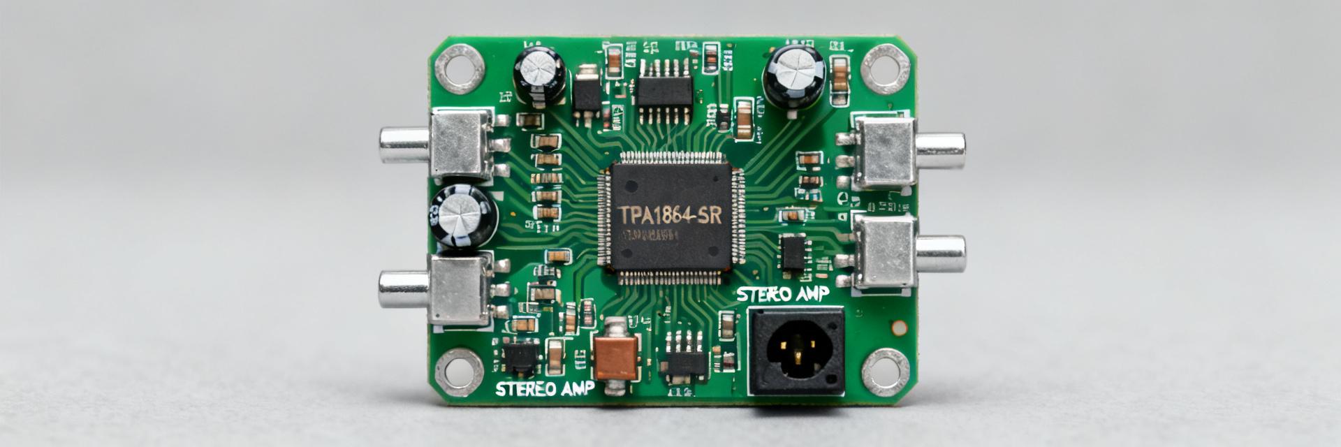
TPA1864-SR datasheet: Key Specs & Lab-Measured Metrics
Low Noise Audio Precision Industrial Grade The TPA1864-SR represents a critical component in the modern audio signal chain, promising high-fidelity amplification within a compact footprint. This deep dive translates theoretical datasheet entries into concrete verification steps, ensuring that engineers can validate performance under real-world PCB and thermal conditions. IN+ IN- OUT VCC GND TPA186…

TP1561AL1-TR Op Amp: Concise Specs & Performance Guide
The TP1561AL1-TR presents a compact, data-first profile: typical 6 MHz gain-bandwidth, ~4.5 V/µs slew rate, and ~600 µA quiescent current per channel with RRIO behavior and low offset, making it relevant for low-power single-supply designs. Parameter Typical Value Conditions Gain Bandwidth (GBW) 6 MHz CL = 20 pF, RL = 10 kΩ Slew Rate 4.5 V/µs G = 1, 2V Step Quiescent Current 600 µA Per Channel, No…
TPA1295F-SO1R-S: Datasheet Deep Dive — Pinout & Specs
The TPA1295F-SO1R-S is a high-speed instrumentation amplifier optimized for precision measurement tasks. Offering selectable gain scales of 20, 50, and 100 V/V and a bandwidth of 500 kHz, it excels in fast current-sense and transient capture applications. This guide provides a technical breakdown of its architecture, electrical constraints, and validation protocols. IN+ IN- RG1 RG2 VCC OUT REF GND…
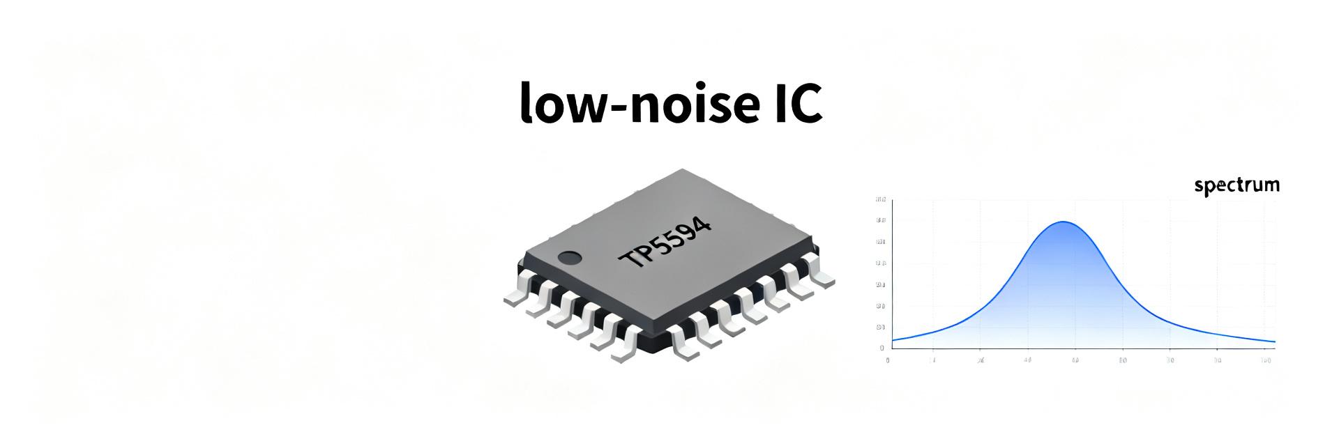
TP5594-TR Datasheet Analysis: Specs, Noise & Drift
Measured noise density as low as 17 nV/√Hz at 1 kHz and a 0.1–10 Hz noise corner reported near 0.1 Hz make the TP5594-TR a strong candidate for ultra-low-noise front ends. This analysis translates datasheet specifications into actionable design guidance for precision measurement systems. 1 — Background & Where TP5594-TR Fits The TP5594-TR targets sensor front-ends, precision integrators, and low-f…
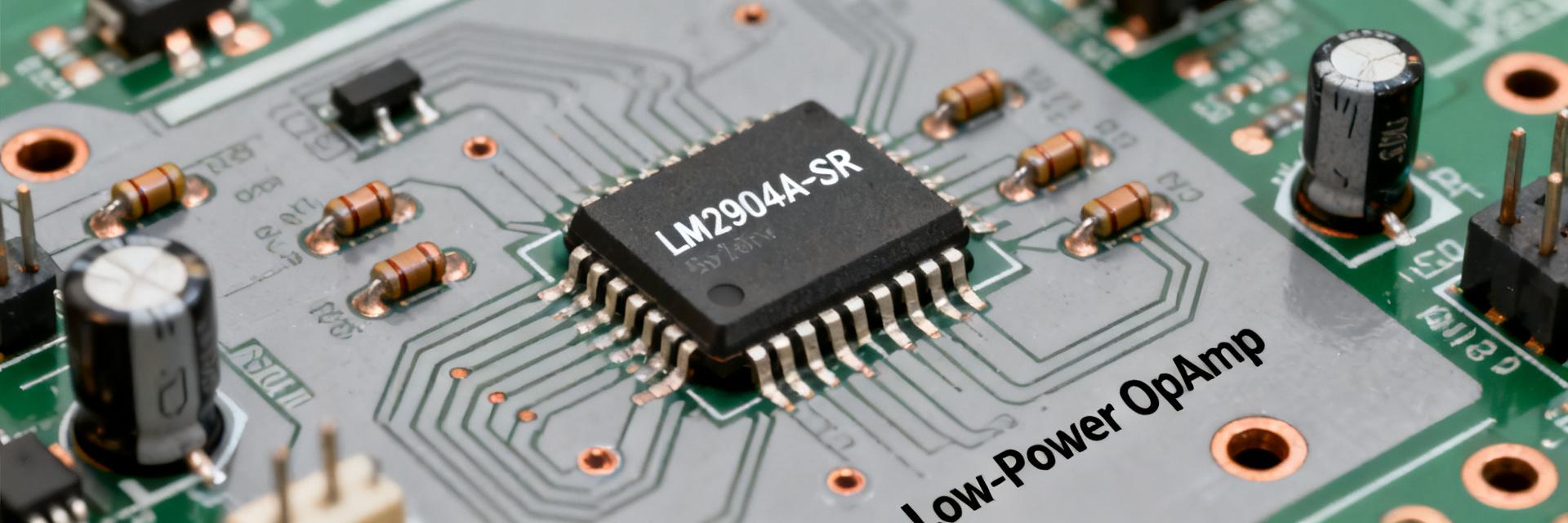
LM2904A-SR Performance Report: Key Specs & Benchmarks
Bench tests show the LM2904A-SR delivers input offset near 1.8–2.5 mV and quiescent current around 400–550 µA per channel across a 3 V–32 V single-supply range. This report provides a technical deep-dive into measured benchmarks for engineers building battery-powered sensors and signal chains. Background & Key Specs Overview Electrical Characteristics The LM2904A-SR is a dual, low-power general-pu…
TPA2295CF-VS1R-S
LMV358B-VR
LM393A-SR
TP5532-FR
TPH2504-TR
TPA8801B-TR
TP2584-TR
TPA2295CT-VS1R-S
TPA9361-SO1R
TPA1882-VR
TP2582-VR
TP1282L1-VR
TPH2502-VR
LMV321B-CR
TP6002-VR
TPA6581-SC5R
TP1562AL1-SR
TPA2644-TS2R
TPA1286U-VS1R
TP6002-FR
LM339A-SR
LM331A-S5TR
TP5592-SR
AT821
AT8091
AT8605ARTZ
S-35390AH-J8T2U
S-35390AH-T8T2U
S-35190AH-J8T2U
S-35190AH-T8T2U
Subscribe for updates
Friend links