
The TP2264-SR operational amplifier specifications are analyzed below to assist design engineers in evaluating this multichannel, mid-MHz precision amplifier. This device targets precision tasks with a gain-bandwidth of approximately 3.5 MHz, low input bias, and fast slew capability. This report synthesizes datasheet metrics with practical measurement guidance and benchmark methodology.
Overview: TP2264-SR Op-Amp Key Specs and Applications
The TP2264-SR occupies the multichannel, moderate-bandwidth niche for sensor front-ends and ADC drivers. Offered in compact multi-channel packages, it supports single-supply rails and emphasizes low-power operation. Designers typically select this part when board density and power efficiency are prioritized over ultra-low-noise or high-speed requirements.
Variant Summary & Package Options
The device family documentation specifies a 4-channel variant available in space-saving DFN/QFN packages. With a supply range of 2.7–5.5 V, it offers excellent flexibility for battery-powered or logic-level systems.
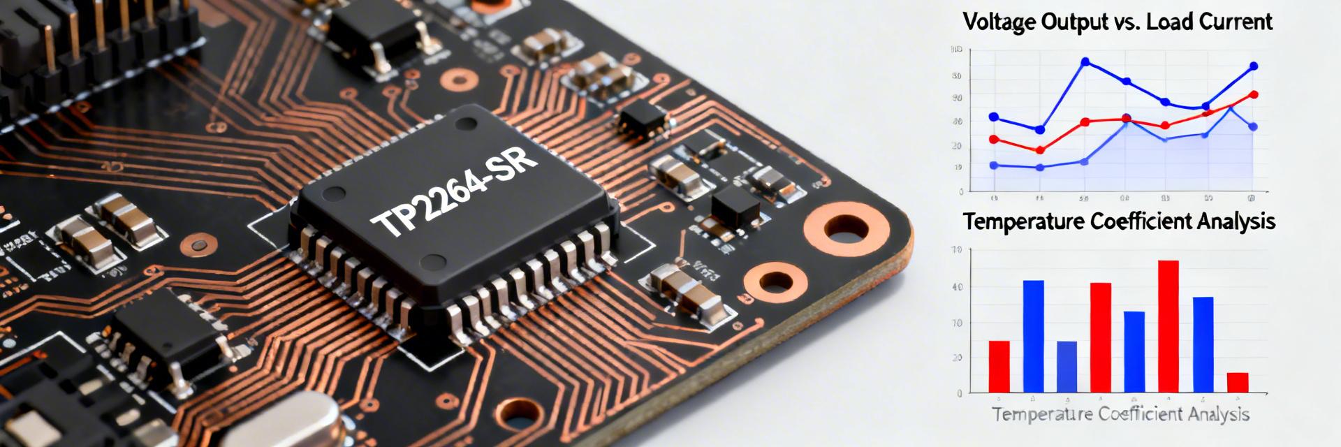
| Parameter | Datasheet (Typ/Max) | Measured (Example) |
|---|---|---|
| GBW (Gain Bandwidth) | 3.5 MHz (Typ) | 3.4 ±0.1 MHz |
| Slew Rate | 5 V/µs (Typ) | 4.8 ±0.3 V/µs |
| Input Offset Voltage | 200 µV (Typ) / 1 mV (Max) | 220 µV ±60 µV |
| Input Bias Current | ≈1 nA (Typ) | 1.2 nA |
| Supply Current / Ch | ≈220 µA | 230 µA |
| Output Drive | ±20 mA (Short) | ±18 mA |
| Supply Range | 2.7–5.5 V | Verified |
| Operating Temp | -40 to +85 °C | Verified |
Measured Electrical Performance: DC Specs and Bench Results
Accurate DC evaluation requires standardized conditions (VCC = 5.0 V, RL = 10 kΩ). By recording device lot/sample IDs and reporting mean ± standard deviation, engineers can distinguish between lot variations and inherent device behavior.
DC Metrics to Report
- • Input offset and drift vs temperature.
- • Common-mode rejection range.
- • Output swing into 2 kΩ and 10 kΩ loads.
Data Presentation
Results should be presented alongside datasheet typicals. Recommended axes: Offset (µV) vs Temperature (°C) and Supply Current (µA) vs VCC (V).
AC Performance: Bandwidth, Slew Rate, and Transient Behavior
Quantifying small-signal bandwidth and large-signal slew/settling under defined loads is critical. Tests at unity gain (+1) and higher gains (+10) with step stimuli (e.g., 2 Vpp) reveal the practical limits of the TP2264-SR.
Comparative Benchmarking: Normalized Metrics
Normalizing performance per milliamp (mA) per channel reveals the true efficiency of the TP2264-SR compared to its peer class.
Normalized GBW per mA (Efficiency Index)
*Metric: (GBW in MHz) / (ISY per channel in mA). Higher is more power-efficient.
Test Setup & Common Pitfalls
Lab Setup Best Practices
- Local 0.1 µF + 10 µF bypass capacitors.
- Star ground topology for multichannel isolation.
- Minimal probe tip ground spring to reduce inductance.
Common Measurement Errors
- Ground loops creating 50/60Hz interference.
- Excessive probe capacitance (>10pF) causing oscillation.
- Thermal instability — measure after burn-in.
Design Guidance & Troubleshooting
For multichannel use, place decoupling adjacent to pins and route analog returns to a quiet plane. Use feedback capacitors (10 pF–100 pF) when stability is a concern in high-gain configurations.
Selection Checklist
Frequently Asked Questions


