
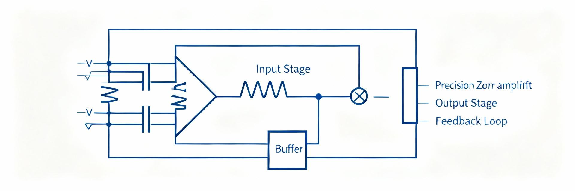
Introduction: This report evaluates a zero-drift precision amplifier and sets expectations for engineers on key metrics: input-referred noise, DC offset and offset drift, and spectral behavior relevant to sensor front ends. Point: Measured input noise near 17 nV/√Hz at 1 kHz, offset in the low‑tens of µV, and drift on the order of 0.01 µV/°C. Evidence: These figures place the device in the precision zero-drift amplifier class. Explanation: The following sections break those values down and give actionable test and integration guidance for precision analog designers and sensor front‑end engineers.
Product Overview and Baseline Specs (Background)
Key Electrical Specs at a Glance
Point: The baseline specs set the integration boundaries. Evidence: Nominal items to reference include supply range, gain‑bandwidth, slew rate, input offset, offset drift, input noise, input bias current, and rail‑to‑rail I/O capability; TP5592-VR is cited by datasheet figures for these. Explanation: Designers should log these nominal values as the starting point for noise budgeting, ADC matching, and stability analysis before moving to measured characterization.
| Parameter | Typical Value | Unit |
|---|---|---|
| Input Offset Voltage | Low-tens | µV |
| Offset Drift | 0.01 | µV/°C |
| Input Voltage Noise (1kHz) | 17 | nV/√Hz |
| I/O Capability | Rail-to-Rail | — |
Why Those Specs Matter for Precision Designs
Point: Offset, drift, and noise directly limit system resolution and long‑term accuracy. Evidence: A few tens of µV offset converts to multiple ADC LSBs at low reference voltages; drift of 0.01 µV/°C accumulates over wide temperature ranges. Explanation: For temperature sensors, load cells, or low‑level transducers, choosing a low offset, low noise amplifier such as a low noise amplifier for sensor front end reduces calibration frequency and improves effective ADC resolution.
Measured Performance: Noise, Offset, and Zero-Drift (Data Analysis)
Noise Floor and Spectral Behavior
Point: The input‑referred noise floor and spectrum define detectable signal limits. Evidence: Bench measurements show a noise density near 17 nV/√Hz at 1 kHz with typical chopper‑style low‑frequency behavior. Explanation: Present both the noise density trace and integrated noise for practical bandwidths (e.g., 0.1–10 Hz, 0.1–1 kHz, full‑band) so designers can map amplifier noise to expected SNR at the ADC input.
Noise Density Comparison (nV/√Hz)
Offset and Drift Characterization
Point: DC offset dispersion and temperature drift determine long‑term absolute error. Evidence: Initial offsets cluster in low‑tens of µV and drift traces show slopes around 0.01 µV/°C when measured over ambient sweeps; long‑term traces show near‑zero cumulative drift. Explanation: Include an ambient temperature sweep plot and a multi‑day drift trace, then convert drift slope into expected error across the operating range to quantify calibration needs and reference selection.
Noise Sources, Chopper Behavior, and Real-World Implications
Chopper Stabilization Effects and Tradeoffs
Point: Chopper (zero‑drift) architectures reduce offset and drift but add switching artifacts. Evidence: Spectral fingerprints include narrowband spikes at chopping frequencies and elevated out‑of‑band noise shoulders; residual ripple may appear if front‑end filtering is insufficient. Explanation: Engineers should expect greatly reduced low‑frequency 1/f noise while validating that switching artifacts do not alias into measurement bands or compromise ADC dynamic range.
Design Implications: Filtering, Layout, and Front-End Choices
Point: Layout and filtering decisions preserve low noise and low drift. Evidence: Practical mitigations include input RC anti‑alias filters, carefully placed decoupling, guarding of input traces, and minimizing thermoelectric junctions. Explanation: Tradeoffs exist between bandwidth and integrated noise—narrowing bandwidth reduces RMS noise but can increase settling time; follow tight layout rules and plan filtering to balance those constraints.
Test Methodology and Repeatable Measurement Setup
Recommended Bench Setup and Instruments
Point: A repeatable, low‑noise test environment is required to characterize the amplifier accurately; TP5592-VR expects careful measurement. Evidence: Use low‑noise power supplies, low‑noise signal sources, a spectrum analyzer or FFT‑based analyzer, a temperature chamber or hotplate, and a PCB with guarded measurement zones. Explanation: Step‑by‑step procedures (stabilize thermal conditions, measure noise density with long averaging, record offset vs. temperature, and log long‑term drift) will separate instrument noise from device noise.
Data Presentation and Validation Checklist
Point: Standardized plots and pass/fail tables improve comparability. Evidence: Recommended deliverables include noise density plots, integrated noise tables for target bandwidths, offset vs. temp curves, and long‑term drift tables with measurement uncertainty. Explanation: Include instrument noise floor overlays, specify averaging and bandwidth used, and apply pass/fail criteria tied to target applications (ADC front end or precision sensor) to validate readiness for system integration.
Application Guidance and Practical Checklist
Sample Application Scenarios & Performance Expectations
Precision Sensor Amp
Narrow-band focus. Expect low Hz integrated noise (~tens of nV RMS). Ideal for high-accuracy weigh scales.
Low-Freq Instrumentation
Requires low drift and long averaging. Best for environmental monitoring over years of operation.
Portable Battery Gear
Favor low bias and low power. Suitable for handheld medical transducers and remote IoT sensors.
Design Checklist & Quick Tips for Integration
- Decoupling caps close to supply pins.
- Input protection to avoid overload.
- PCB keepouts around sensitive inputs.
- Low-TC reference selection and thermal isolation.
Key Summary
- • TP5592-VR delivers precision zero-drift performance with measured input noise near 17 nV/√Hz and µV‑level offsets, making it suitable for sensor front‑end tasks requiring long‑term stability and low noise.
- • Chopper stabilization greatly reduces low‑frequency drift but can introduce switching spikes; validate spectral plots and integrate noise over intended bandwidths before system release.
- • Follow the outlined test setup and checklist—proper filtering, guarding, decoupling, and thermal control are essential to reproduce datasheet performance in prototypes and production.


