The official datasheet highlights rail-to-rail I/O, low quiescent current, and stable high-frequency response for the TPA6531-SC5R — key metrics that determine suitability for low-voltage sensor and portable-audio designs. This report converts those claims into practical, testable implications engineers can use during component selection and bench validation.
Goal: A clear, testable breakdown of core op-amp specs, how they translate to measured system performance, and a compact selection & test checklist for single-supply, battery-powered designs.
Background: Where TPA6531-SC5R Fits in Low‑Voltage Op Amp Designs
Key architectural features to highlight
The device uses a CMOS rail-to-rail input/output architecture and targets single-supply, low-voltage systems. Typical package and operating-temperature range are documented in the official datasheet. Below is a compact feature-implication summary for quick design triage.
Feature
Short Implication
Rail-to-rail I/O
Maximizes dynamic range on low supplies; eases level-shifting for sensors
Low quiescent current
Suitable for battery-powered systems; reduces standby draw
CMOS process
Low input bias, good for moderate source impedances; watch input ESD limits
Typical application domains and target systems
Common targets include sensor front-ends, portable audio preamps, and single-supply instrumentation. For sensors, input range and bias current dominate; for audio, slew-rate, THD and output swing matter. Use long-tail searches such as "low-voltage op amp use cases" to benchmark competing topologies.
Core DC Specs — Input & Output Characteristics
Inputs: offset, bias current, common‑mode range
Input offset and bias current set static measurement error. If Vos (typ) = Vos_typ and input bias = Ib_typ, the worst-case DC error for a 100kΩ source is:
Core AC Specs & Stability — Bandwidth, Slew, Noise
Frequency Response
GBW and slew rate determine usable closed-loop gain. For a target f_sig, the max gain is GBW / f_sig. Slew rate limits peak undistorted amplitude at high frequency.
Noise & Distortion
Input-referred noise guides precision tradeoffs. Use the datasheet’s recommended output decoupling (10–100 nF) when driving cables to maintain phase margin.
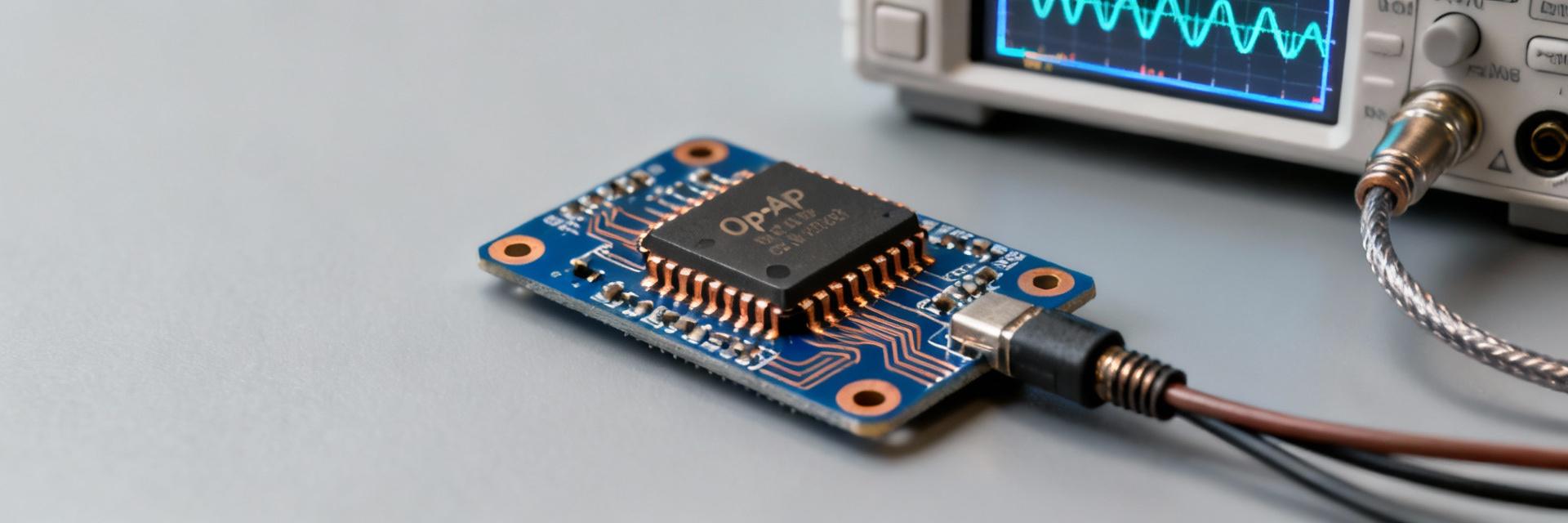
Practical Evaluation & Bench Test Methods
Essential bench tests and pass/fail criteria
✓DC offset versus temperature: Compare against datasheet max limits.
✓Gain‑bandwidth: Sweep sine wave to find the -3dB point.
✓Slew‑rate: Use large-step pulse and measure ΔV/Δt.
Interpreting discrepancies: common measurement pitfalls
Common causes for deviation include poor PCB layout, insufficient supply decoupling, and probe loading. Remedies include local decoupling within 5 mm of the V+ pin and using 10–100 nF bypass capacitors.
Comparison Scenarios & Example Designs
Sensor Front‑End
For high-impedance temperature sensors, Vos and Ib are critical. If Ib × Rs approaches Vos, select lower-bias variants or add input buffering to maintain signal integrity.
Audio Preamp
Choose closed-loop gain so GBW/f_sig ≥ 10× safety margin. Verify THD at peak amplitude and check headroom from the datasheet output-swing curve to prevent clipping.
Design Recommendations & Selection Checklist
When to Choose
Rail-to-rail I/O required
Battery-sensitive operations
Moderate bandwidth needs
PCB Best Practices
Caps close to supply pins
Short, shielded input traces
Guard rings for high-Z inputs
Summary
1
Rail‑to‑rail I/O and low quiescent current make this op amp ideal for portable sensors; always verify numeric margins against final power budgets.
2
Compute Offset + (Ib × Rs) error and map GBW to required gain to ensure the design avoids non-linear regions or clipping.
3
Follow a strict bench checklist: DC offset, noise spectrum, and capacitive-load stability are non-negotiable for production-ready designs.
Frequently Asked Questions
What are the essential measurements in a TPA6531-SC5R test procedure?
+
Essential measurements include DC offset vs. temperature, input bias with a known source resistance (e.g., 100kΩ), gain‑bandwidth sweep, slew‑rate via fast step, noise spectrum, and output swing/load testing. Each measurement should be performed with proper decoupling and controlled probe loading.
How should designers estimate battery life from the op amp specs?
+
Estimate battery life by summing the quiescent currents of all active analog blocks and dividing battery capacity (mAh) by total current (mA). Use the formula: Life_hours ≈ Battery_mAh / I_total_mA. Include duty-cycle factors for burst or shutdown modes.
What layout or test fixes resolve discrepancies versus datasheet specs?
+
Start with improved decoupling (10–100 nF plus 1 µF), shorten sensitive traces, add series output resistors for capacitive loads, and use buffering for high‑impedance inputs. In testing, verify probe capacitance and grounding; use differential probing for AC tests.