
The LM2904A-TSR is a low‑power dual operational amplifier designed for single‑supply and battery applications; its typical datasheet range spans roughly 3 V to 36 V, with quiescent current figures on the order of 100 μA per channel and an input common‑mode that includes ground. This quick read uses those key specs to show where the part fits, what to test on the bench, and practical design cautions for engineers focused on dependable, low‑power analog front ends.
Background & Key Identifiers (Background introduction)
What the LM2904A-TSR is (device class & core features)
Point: The device is a dual general‑purpose operational amplifier optimized for low quiescent current and single‑supply operation. Evidence: The official datasheet lists low supply current per channel, input common‑mode to ground, and substantial open‑loop gain. Explanation: These specs make the LM2904A-TSR attractive for battery‑powered sensor front ends and reference amplifiers where power budget and rail‑to‑ground sensing are primary constraints rather than ultra‑low noise or high bandwidth.
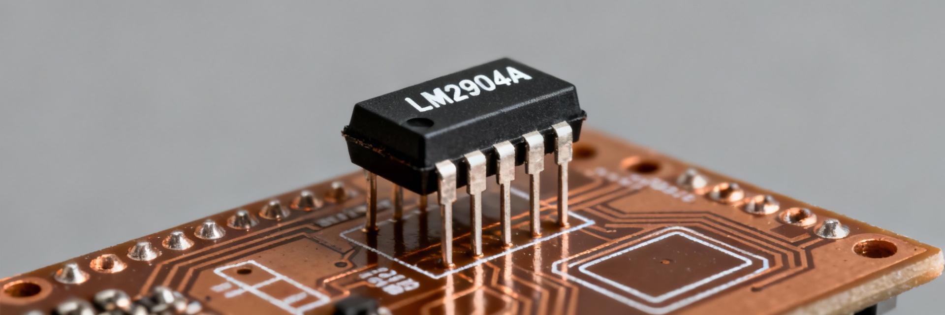
Package, pinout & temperature grades at a glance
Point: Common -TSR suffix variants target compact surface‑mount packages. Evidence: Typical offerings include TSSOP or PDSO surface‑mount packages with standard 8‑pin dual‑op amp pinouts and mounting suited for automated assembly. Explanation: Designers should verify pin mapping and thermal pad options for their PCB, and expect operating ranges commonly spanning roughly −40 °C to 125 °C for industrial grades when planning for elevated ambient or enclosed applications.
Electrical Specifications — quick specs table + highlights (Data analysis)
Power & output specs to call out
Point: Key power and output metrics drive suitability for single‑supply, low‑power systems. Evidence: Expect single‑supply operation from around 3 V up to approximately 36 V, quiescent current near 100 μA per channel, modest output drive (tens of mA), and output swing that does not reach true rails. Explanation: Verify absolute maximum ratings for supply and input voltages, allow margin from rails for expected output swing, and plan for external pull‑up/pull‑down or drivers when larger load currents are required.
| Parameter | Typical | Design note |
|---|---|---|
| Supply range | ~3 V – 36 V | Use split ± supplies equivalently when needed |
| Quiescent current | ~100 μA / channel | Good for battery life; watch total budget |
| Output drive | tens of mA | Not intended for heavy loads |
| Output swing | Rail‑limited | Plan headroom from rails |
Input & DC characteristics to monitor
Point: DC input parameters determine precision and biasing needs. Evidence: Designers should consult offset voltage (typical vs maximum), input bias current, input common‑mode range that includes ground, and CMRR/PSRR figures in the datasheet. Explanation: Offset and bias currents affect low‑frequency accuracy and drift; CMRR and PSRR inform layout and supply filtering choices when measuring small differential signals near ground in single‑supply topologies.
Performance & Frequency Response (Data analysis)
AC behavior: bandwidth, slew rate, stability
Point: AC metrics set closed‑loop gain and transient limits for the amplifier's performance. Evidence: Unity‑gain bandwidth and slew rate on this class of amplifier are modest compared with high‑speed op amps, and phase margin is balanced for stability in common closed‑loop gains. Explanation: For closed‑loop gains of 1–10 the amplifier behaves predictably, but designers requiring higher closed‑loop bandwidth or fast edge reproduction should evaluate the LM2904A-TSR performance against desired gain‑bandwidth product and consider alternate parts for higher performance.
Noise, distortion & thermal behavior
Point: Noise and distortion are moderate; thermal drift impacts offset over temperature. Evidence: Input‑referred noise and THD at small signal levels are adequate for many sensor and control loops but not optimized for precision audio or low‑noise instrumentation. Explanation: Account for offset drift with temperature derating in critical DC paths, and include local filtering or calibration to mitigate cumulative noise and distortion effects in precision measurement chains.
Typical Application Circuits & Design Tips (Method/guide)
Common circuits (voltage follower, single‑supply amplifier, comparator alternative)
Point: Typical use cases are simple unity‑gain buffers, single‑supply amplifiers, and comparator replacements in low‑speed designs. Evidence: Wiring as a buffer or non‑inverting amplifier yields stable behavior if inputs remain within common‑mode range and outputs are not forced to rail. Explanation: Avoid relying on rail‑to‑rail output performance; for comparator roles, add hysteresis and ensure input thresholds stay away from rail margins to prevent undefined switching or saturation recovery delays.
Layout, decoupling and compensation tips
Point: PCB layout and decoupling significantly affect measured performance. Evidence: Place supply decoupling capacitors near the device supply pins (0.1 μF ceramic plus 1 μF electrolytic), keep input traces short, and add series resistors for input protection when transients are possible. Explanation: Proper placement reduces PSRR and CMRR degradation, preserves stability, and minimizes noise coupling into sensitive inputs; consider small compensation networks for specific closed‑loop pole shaping when oscillation is observed.
Practical Benchmarks & Test Procedures (Data-driven / case)
Essential tests to validate performance
Point: Targeted bench tests confirm the datasheet behavior in your system context. Evidence: Recommended tests include DC offset and drift (idle, then warmed), gain accuracy with known sources, output swing under expected load, slew rate via step input, and PSRR/CMRR by injecting supply or common‑mode variations. Explanation: Use known thresholds (offset within datasheet max, output margin > few hundred mV from rails under load) to pass or fail, and log temperature dependence to verify operating envelopes.
Typical expected results & "red flags"
Point: Clear pass/fail criteria speed debug. Evidence: Expect offset within datasheet max, quiescent current near typical figure, output swing margin measurable from rails, and slew rate matching order‑of‑magnitude in the datasheet. Explanation: Red flags include excessive offset or drift, quiescent current far above typical (shorts or thermal issues), output stuck at rail, or oscillation—remedies include layout fixes, decoupling, input protection, and replacing marginal parts.
Design Comparison & Quick Selection Checklist (Actionable)
When to choose the LM2904A-TSR — tradeoffs
Point: Choose this amplifier when low quiescent current, wide single‑supply range, and ground‑referenced inputs outweigh the need for high bandwidth or rail‑to‑rail outputs. Evidence: Its balance of low supply current and practical analog performance suits battery sensors, watchdog circuits, and slow ADC drivers. Explanation: If requirements demand higher slew rate, lower noise, or true rail‑to‑rail outputs, select a part optimized for those metrics instead of this general‑purpose low‑power device.
Quick selection checklist for engineers
Point: Use a concise procurement checklist to match part to requirement. Evidence: Include supply range, max quiescent current, required output drive, operating temperature, package type, input common‑mode needs, DC precision (offset/ bias), and AC needs (bandwidth/slew). Explanation: Copy these bullets into design docs to quickly filter candidate amplifiers and ensure the LM2904A‑TSR meets the system's electrical and mechanical constraints before prototyping.
Summary
- The LM2904A-TSR is a low‑power dual op amp positioned for single‑supply and battery applications; verify supply range, quiescent current, and input common‑mode against system needs before selection.
- Key specs to confirm on the bench are DC offset/drift, output swing under load, and basic AC metrics such as slew rate and unity‑gain behavior to validate expected performance.
- Design cautions include non‑rail‑to‑rail output swing, modest bandwidth, and sensitivity to layout; good decoupling and short input traces mitigate many common issues—download the official datasheet and run the essential tests listed above.


