The TPA2295CF-VS1R-S is a compact current-sense amplifier optimized for precision shunt monitoring, offering a broad supply range, selectable gains, and modest bandwidth suitable for power-management telemetry and motor-control sensing. This datasheet-oriented guide highlights supply and thermal limits, available gains and bandwidth, and pinout/PCB integration details to accelerate engineering screening and prototype fit decisions.
1 — Product overview & quick specs (background)
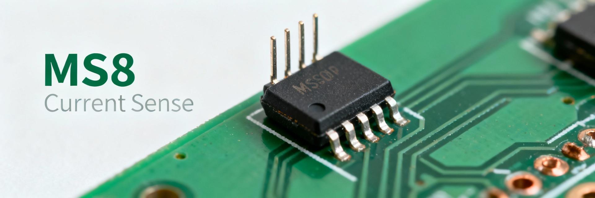
1.1 Key specs snapshot (table + bullets)
Point: Engineers need an at-a-glance specs snapshot to screen parts quickly. Evidence: Typical screening values below capture the electrical and mechanical parameters used in BOM filters. Explanation: Use these numbers for quick pass/fail in system-level selection before detailed bench evaluation.
| Parameter | Value / Notes |
|---|---|
| Supply voltage | Single-supply ~3.3–5.5 V (use conservative margin) |
| Temperature range | Industrial-grade junction range; verify derating for reliability |
| Gain options | Selectable: 20, 50, 60, 100, 200 V/V |
| Bandwidth | Bandwidth up to ~0.5 MHz (gain-dependent) |
| Package | 8-pin MSOP/TSSOP-style variants |
| Quiescent current | Low μA to low mA range depending on mode |
| Input/common-mode | Wide common-mode around ground to supply limits |
| Output | Single-ended voltage scaled to sense resistor |
Point: Quick bullets summarize screening criteria. Evidence: Values above reflect typical electrical expectations engineers use. Explanation: Use gain and bandwidth tradeoffs to decide whether precision or transient response dominates the application.
- Supply margin: design for at least 10% headroom below absolute limits.
- Gain selection: higher gains improve sensitivity but reduce bandwidth and increase offset impact.
- Package choice: pick footprint variant matching thermal and assembly constraints.
1.2 Functional role & typical application domains
Point: The device is a current-sense amplifier for shunt-based measurement. Evidence: It replaces discrete op-amp sensing stages with an integrated gain and input-conditioning path. Explanation: Typical use cases include shunt monitoring in power supplies, battery management, motor current feedback, and overcurrent protection where precision and compact PCB footprint matter.
2 — Pinout & package details (pinout)
2.1 Pin-by-pin table and symbol mapping
Point: Accurate net naming avoids schematic/BOM errors. Evidence: The pinout table below maps pin numbers to functions and recommended net names for clear schematic symbols. Explanation: Include these names in the BOM and PCB silk to simplify review and test fixture wiring; this paragraph also references the pinout in the mechanical drawing.
| Pin | Name | Function | Recommended net |
|---|---|---|---|
| 1 | IN+ | Non-inverting sense input | SHUNT_P |
| 2 | IN- | Inverting sense input | SHUNT_N |
| 3 | GAIN | Gain select / mode | GAIN_SEL |
| 4 | V+ | Supply | VCC |
| 5 | OUT | Amplified output | ISENSE_OUT |
| 6 | GND | Ground / reference | GND |
| 7 | NC | No connect / keepout | - |
| 8 | PAD | Exposed pad (if present) | PAD_GND |
2.2 Package dimensions & recommended land pattern
Point: Footprint tolerances and solder fillet guidance reduce assembly defects. Evidence: Typical 8-pin MSOP/TSSOP outlines use 0.65–0.8 mm pad pitch and exposed pad options. Explanation: Keep short thermal vias under the exposed pad, provide 4–6 mil solder mask relief, and add 0.1–0.2 mm clearance from adjacent copper to avoid solder bridging.
3 — Absolute maximum ratings & recommended operating conditions (data analysis)
3.1 Absolute maximum ratings table
Point: Respect absolute limits to avoid permanent damage. Evidence: The official datasheet lists supply, input, output, and junction temperature limits; exceeding these risks latch-up or ESD failures. Explanation: Treat absolute values as strict cutoffs and design clamp circuits and PCB creepage distances to prevent transient excursions into these regions.
| Parameter | Absolute max / note |
|---|---|
| Supply voltage | Do not exceed supply absolute max; design clamps for transients |
| Input pin voltage | Input range vs. supply; avoid drive beyond rails |
| Output short | Limit duration per thermal time constants |
| Junction temperature | Observe Ta/Tj limits and derate per thermal path |
3.2 Recommended operating range + derating guidance
Point: Choose conservative operating margins for reliability. Evidence: Recommended ranges in the datasheet indicate safe supply and temperature windows and specific decoupling values. Explanation: Apply 10–20% derating to supply headroom, use recommended decoupling near V+, and add snubbing or input clamps for high-energy transients.
4 — Electrical characteristics & performance (data deep-dive)
4.1 DC electrical parameters to test and specify
Point: Critical DC specs determine measurement accuracy. Evidence: Key items include gain accuracy, input offset and offset drift, input bias, input common-mode range, and quiescent current. Explanation: Specify typical and maximum tolerances, measure offset drift across temperature, and ensure ADC input scaling accounts for offset and gain error.
4.2 AC/transfer performance and graphs to include
Point: AC behavior defines transient measurement fidelity. Evidence: Important plots are gain vs frequency, phase margin, slew rate, noise spectral density, CMRR and PSRR. Explanation: Generate gain-vs-frequency at each gain setting, test stability with expected source capacitance, and include output swing vs load plots for ADC interface planning.
5 — Typical application circuits & design examples (case)
5.1 Single-supply current-sense reference design (schematic + part values)
Point: A reference design speeds prototype verification. Evidence: Example values below show sense resistor selection and output scaling math. Explanation: Choose Rsense to produce a practical Vshunt at expected max current (Vshunt × gain = ADC full-scale margin), add 0.1 μF decoupling at V+, and include input RC for filtering.
| Item | Example |
|---|---|
| Rsense | 100 μΩ–10 mΩ depending on current |
| Decoupling | 0.1 μF + 1 μF close to V+ |
| Input RC | R=10–100 Ω, C=10–100 nF for anti-aliasing |
5.2 Protection, filtering & interface examples
Point: Protection prevents field failures. Evidence: Use series R and clamp diodes or TVS at inputs, plus RC anti-aliasing to limit bandwidth. Explanation: Ensure protection networks keep common-mode and differential voltages within allowed ranges; buffer outputs into ADC inputs if ADC sampling capacitance causes instability.
6 — PCB integration, testing & troubleshooting (actionable)
6.1 PCB layout checklist and thermal/EMC tips
Point: Layout impacts measurement accuracy and EMC. Evidence: Short sense traces, solid ground returns, and decoupling close to V+ reduce noise and error. Explanation: Route shunt traces with wide copper, use star ground for the amplifier reference, place decoupling within 1–2 mm of supply pin, and add thermal vias beneath exposed pad if present.
6.2 Test procedures & common failure modes
Point: A concise test plan catches common defects. Evidence: Bench steps include DC sanity checks, gain verification with known Rsense, frequency sweep, and noise measurement. Explanation: Probe with low-capacitance clips, verify output scaling against calculations, and if offset or oscillation appears, check layout, source capacitance, and input protection interactions.
Summary
The guide condenses the essential items engineers need to assess the TPA2295CF-VS1R-S for shunt-sensing applications: supply and thermal limits, selectable gains with bandwidth impacts, pinout/footprint considerations, and practical PCB and test best practices. Verify absolute operating limits in the official datasheet during final qualification and follow the layout and protection checklists before prototype runs.
Key summary
- Primary screening: use supply, gain, and bandwidth values to decide fit; verify Rsense and ADC scaling early to avoid redesigns.
- Pinout and footprint: follow recommended pad pitch and exposed-pad thermal vias; name nets consistently (SHUNT_P/SHUNT_N, ISENSE_OUT).
- Reliability checks: respect absolute maximums from the datasheet, apply 10–20% derating, and include input protection and decoupling for field robustness.
FAQ
What are the typical gain options and how do they affect bandwidth for TPA2295CF-VS1R-S?
Typical selectable gains are 20, 50, 60, 100, and 200 V/V. Higher gains increase sensitivity but reduce usable bandwidth and can amplify offset and noise. For fast transient sensing prefer lower gain settings or add downstream digital scaling; always verify gain-vs-frequency plots for each selected gain.
How should I implement the pinout in my schematic to avoid wiring errors?
Use explicit net names as shown in the pin table (e.g., SHUNT_P, SHUNT_N, ISENSE_OUT, VCC, GND). Place decoupling capacitors close to V+ and label the exposed pad as PAD_GND with thermal vias. Consistent naming simplifies BOM review and prevents misrouting during layout and test fixture wiring.
What bench tests should validate performance before system integration?
Run a DC sanity check (no-load supply and output), measure gain using a known Rsense at multiple currents, sweep frequency to capture gain-vs-frequency, and measure noise with proper filtering. Use low-capacitance probe tips, verify offsets across temperature, and confirm protection clamps do not distort measurements.
