
The LM393A-SR datasheet hides the handful of numbers that decide whether the comparator will survive and behave in your system: a usable supply range around 2.0–36 V single-supply, quiescent current in the low hundreds of microamps per comparator, and input offset voltages on the order of a few millivolts. These figures set thresholds, power budget, and accuracy limits for battery-powered monitors, simple ADC front-ends, and threshold detectors. This guide is a practical, number-focused walkthrough of the datasheet so you can extract the right specs and apply them to real designs without reading every page of the full datasheet.
Start by scanning supply limits, input common-mode range, offset and bias, output sink capability and VCE(sat), propagation delay, and absolute maximums. The following sections explain what each number means, how to calculate margins, and how to verify the specs on the bench.
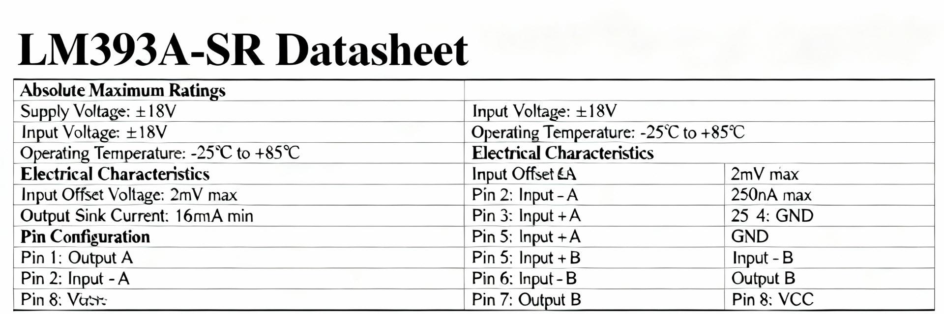
1 — What the LM393A-SR is and why its datasheet matters (Background)
Part family & core function
Point: The LM393A-SR is a low-power voltage comparator family member with open-collector outputs, typically implemented as dual comparators in one package. Evidence: Comparator families use differential inputs and open-collector outputs to interface cleanly with pull-ups to various logic domains. Explanation: Open-collector outputs allow mixed-voltage interfacing and wired-OR arrangements, making these comparators suitable for power monitoring, zero-cross detection, and simple thresholding in sensor front-ends where isolation of output pull-up voltage is useful.
Which datasheet numbers determine fit for purpose
Point: Scan a short list of numeric specs first in any datasheet: supply voltage range, input common-mode range, input offset (typical and max), propagation delay, output sink current and VCE(sat), quiescent current, and absolute maximums. Evidence: These values directly control accuracy, timing, and reliability under expected loads and temperatures. Explanation: Prioritizing these specs avoids surprises—if offset drift or common-mode limits violate your thresholds, the comparator will misfire regardless of other attractive features; similarly, supply current and VCE(sat) determine battery life and logic-compatibility.
2 — Key electrical specs of the LM393A-SR at a glance (Data analysis)
Supply & power specs (VCC ranges, max ratings, quiescent current)
Point: The datasheet reports usable single-supply ranges near 2.0–36 V and typical supply current per comparator in the hundreds of microamps; absolute maximum VCC is higher and must be respected. Evidence: Typical family values show single-supply operation that enables wide-range battery and industrial supplies; quiescent current is low enough for many battery designs. Explanation: For battery systems, calculate battery life by multiplying total device quiescent current by battery voltage and capacity; for mixed-voltage systems, the open-collector outputs allow pull-ups to logic rails up to the comparator's allowed pull-up voltage, but never exceed absolute max supply or input pin ratings.
Input characteristics (offset, bias, common-mode range)
Point: Key input numbers include input offset voltage (typical and max), input bias/current, and common-mode range relative to the rails. Evidence: Input offset commonly measures a few mV typical, worse at extremes and over temperature; input common-mode often includes ground but does not always include the positive rail. Explanation: The input offset voltage LM393A-SR determines threshold accuracy: a nominal 3 mV offset shifts your trip point by that voltage, while input bias current interacting with source impedance introduces additional error. Always check typical versus worst-case offset and include temperature drift in margining.
3 — Output behavior and timing numbers (Data analysis)
Output drive, saturation and pull-up design
Point: Open-collector outputs require an external pull-up; datasheet gives VCE(sat)/VOL at specified sink currents and a maximum recommended sink current in milliamps. Evidence: Typical VCE(sat) increases with sink current; datasheet examples show safe sink currents that keep VCE(sat) low. Explanation: Choose pull-up R using R = (Vpull-up - VIL) / Isink_required. Example: for 3.3 V logic, required low level VIL = 0.4 V and expected sink 4 mA → R ≈ (3.3 - 0.4) / 4 mA ≈ 725 Ω. Round to 820 Ω and confirm VCE(sat) at that sink current from the datasheet to ensure the low level stays within logic thresholds.
Propagation delay & response characteristics
Point: Propagation delay and rise/fall times depend on supply voltage, load capacitance, and pull-up resistor; datasheet lists typical and maximum propagation delays. Evidence: With weak pull-ups and larger load capacitances, rise time grows and effective propagation time to logic threshold increases. Explanation: The comparator is suitable for kHz-range threshold detection but not high-speed logic edges; use the timing specs to judge suitability. See the timing table below comparing typical vs. worst-case delays under standard test conditions.
| Parameter | Typical | Max (worst-case) |
|---|---|---|
| Supply range (single) | 2.0 V – 36 V | Absolute max per datasheet |
| Quiescent current per comparator | ~200–300 μA | Specify max from datasheet |
| Input offset (typ / max) | ~2–5 mV / up to tens of mV | See datasheet tolerance |
| Propagation delay (typ / max) | ~1 μs | Several μs under worst load |
| Output sink | tens of mA capability | Ensure VCE(sat) spec at chosen sink |
4 — Thermal, absolute maximums and reliability numbers (Method guide)
Absolute maximum ratings & safety margins
Point: Absolute maximums (max VCC, input pin voltages, storage temperature) are non-negotiable; design using derated limits (commonly 70–80% of absolute max). Evidence: Datasheet lists absolute maximums to protect against catastrophic failure. Explanation: Convert absolute max to safe operating limits by applying a derating factor—e.g., limit continuous supply to 70% of absolute maximum for long-term reliability, and specify transient protection for brief excursions beyond normal operating range.
Thermal resistance, package limits, and temperature ranges
Point: Use junction-to-ambient thermal resistance (θJA) and package power dissipation to calculate worst-case junction temperature. Evidence: Datasheet provides θJA and maximum junction temperature; combine with ambient and power dissipation to check thermal headroom. Explanation: For a comparator toggling with repeated sink currents, compute Pdiss ≈ Isink × VCE_avg + ICC × VCC. Worst-case junction Tj = Ta + Pdiss × θJA. If Tj approaches limits, add copper area or use forced airflow to reduce θJA.
5 — How to interpret LM393A-SR datasheet numbers in real designs (Method guide)
Margining and worst-case calculations
Point: Combine offset, bias, tolerance, and temperature drift to derive worst-case threshold error; use simple stacking and root-sum-squares where appropriate. Evidence: Example calculation below demonstrates method. Explanation: Worked example: desired threshold 100 mV, input offset worst-case = 10 mV, temp drift = 5 mV, bias-induced error = 2 mV → worst-case error = 10 + 5 + 2 = 17 mV. Specify margin (e.g., 3× worst-case) or adjust comparator threshold to compensate in design and test plans.
Example design snippets (pull-ups, hysteresis, input protection)
Point: Practical snippets include pull-up selection, hysteresis resistor equations, and input clamp strategies. Evidence: Pull-up R example above; hysteresis using positive feedback: Vhyst ≈ (Vout_high - Vout_low) × R1/(R1+R2) for discrete ratios. Explanation: For chatter prevention, choose R values producing a few millivolts to tens of millivolts of hysteresis relative to expected noise. For inputs that may exceed rails, use series resistors and clamp diodes to limit input currents within datasheet pin limits.
6 — Bench validation checklist, common pitfalls and selection tips (Case / action)
Quick bench tests to verify datasheet claims
Point: Run a short set of lab checks: measure quiescent current, verify input offset, measure propagation delay, and test output saturation under expected sink loads. Evidence: Use a precision source, high-resolution DMM, and an oscilloscope with a known input step and pull-up network. Explanation: Measure ICC with no load, then with pull-up in place; compare offset measured across temperature extremes to datasheet worst-case; time propagation from input step to output crossing using an oscilloscope; document tolerances in the test plan.
Troubleshooting & when to pick a different comparator
Point: Common failures stem from violating common-mode range, insufficient pull-up, or thermal overstress. Evidence: Symptoms include stuck outputs, incorrect thresholds, and slow edges. Explanation: If you need rail-to-rail input or lower offset, or nanosecond-scale propagation, choose a different family. Update the datasheet checklist and comparator specs matrix to include these selection rules before finalizing the BOM.
Key summary
- Check supply range and absolute maximums first: ensure operating VCC stays well inside datasheet limits to prevent damage and margin errors; this avoids many early design failures.
- Input offset, bias and common-mode range determine threshold accuracy; include worst-case offset and temperature drift in threshold margin calculations to guarantee performance.
- Open-collector outputs require pull-up selection based on VCE(sat) and sink currents; calculate Rpull-up to meet logic-level low and speed requirements.
- Use thermal numbers (θJA and Pdiss) to compute worst-case junction temperature and add cooling or derate if necessary for reliable long-term operation.
Common questions
How do I verify LM393A-SR quiescent current on the bench?
Measure supply current with a microamp-resolution meter in series with VCC, with outputs unloaded and inputs mid-rail; expect currents near datasheet typical values, allow margin for variation across temperature, and document both typical and worst-case measurements.
What pull-up resistor should I use for LM393A-SR with 3.3 V logic?
Calculate R = (Vpull-up - VIL) / Isink_required. For 3.3 V logic, VIL = 0.4 V and desired sink 4 mA gives R ≈ 725 Ω; select the next standard value (820 Ω) and verify VOL at that sink current against the datasheet VCE(sat).
When should I replace the LM393A-SR with a different comparator?
Choose a different family if you need rail-to-rail inputs, lower offset (microvolt-level), or faster propagation (sub-microsecond) than the datasheet lists; use comparator specs and your timing/accuracy requirements as decision criteria.
Summary
Recap: the design-critical numbers are supply range, input offset and bias, input common-mode range, output sink current and VCE(sat), propagation delay, and thermal/absolute maximums. Always cross-check these figures in the manufacturer datasheet and run the quick bench checklist before committing to the part to avoid late-stage surprises when integrating the LM393A-SR into your product.


