
The article opens with a data-driven snapshot: this precision zero-drift amplifier advertises input offset ≤10 µV, drift ≈0.008 µV/°C, 0.1–10 Hz noise ≈1.1 µVpp, quiescent current ≈34 µA per amplifier, ~350 kHz bandwidth, and rail-to-rail I/O over a wide supply range. These published figures set the acceptance targets designers must preserve through pinout interpretation, footprint choice, and PCB layout to reach sensor-grade performance.
Background & Key Specs at a Glance
One-line spec summary to lead the article
Point: Provide a compact reference so designers can quickly screen suitability. Evidence: Key published numbers above form the quick accept criteria. Explanation: The following spec box condenses the headline figures so electrical or battery-constrained applications can validate fit before detailed layout work.
| Parameter | Value / Notes |
|---|---|
| Input offset | ≤10 µV |
| Offset drift | ≈0.008 µV/°C |
| Low-frequency noise (0.1–10 Hz) | ≈1.1 µVpp |
| Quiescent current | ≈34 µA per amp |
| Bandwidth (small-signal) | ≈350 kHz |
| IO | Rail-to-rail input/output |
| Supply range | Wide; see datasheet for min/max |
| Packages | DFN/QFN/WLCSP options |
Primary use-cases and performance niche
Point: Identify where the device provides the most value. Evidence: Extremely low offset, near-zero drift, and low 0.1–10 Hz noise prioritize DC accuracy and long-term stability. Explanation: This combination suits precision sensors, low-power battery telemetry, and instrumentation front-ends where microvolt-level drifts dominate system error and quiescent current impacts battery life.
Electrical Specifications Deep-Dive (from the TP5532-FR datasheet)
Input & output performance: offsets, noise, CMRR, input range
Point: Interpreting offset and drift reveals practical error budgets. Evidence: Offset ≤10 µV and drift ≈0.008 µV/°C are typical-dominant specs; low-frequency noise ≈1.1 µVpp is measured over 0.1–10 Hz. Explanation: Designers should use the datasheet test conditions (ambient temperature, specified supply rails, and defined load) when comparing lab results; RMS vs. peak-to-peak reporting affects perceived noise margin for DC measurements.
Power, bandwidth & dynamic behavior
Point: Power and dynamic specs determine battery life and signal fidelity. Evidence: Quiescent current ≈34 µA per amplifier and ~350 kHz bandwidth imply low-power yet moderately wide small-signal response. Explanation: Expect longer battery life with single-supply operation; reproduce datasheet bandwidth with light loads, bypass capacitors close to V+ and V–, and proper scope probe compensation when validating slew and closed-loop stability.
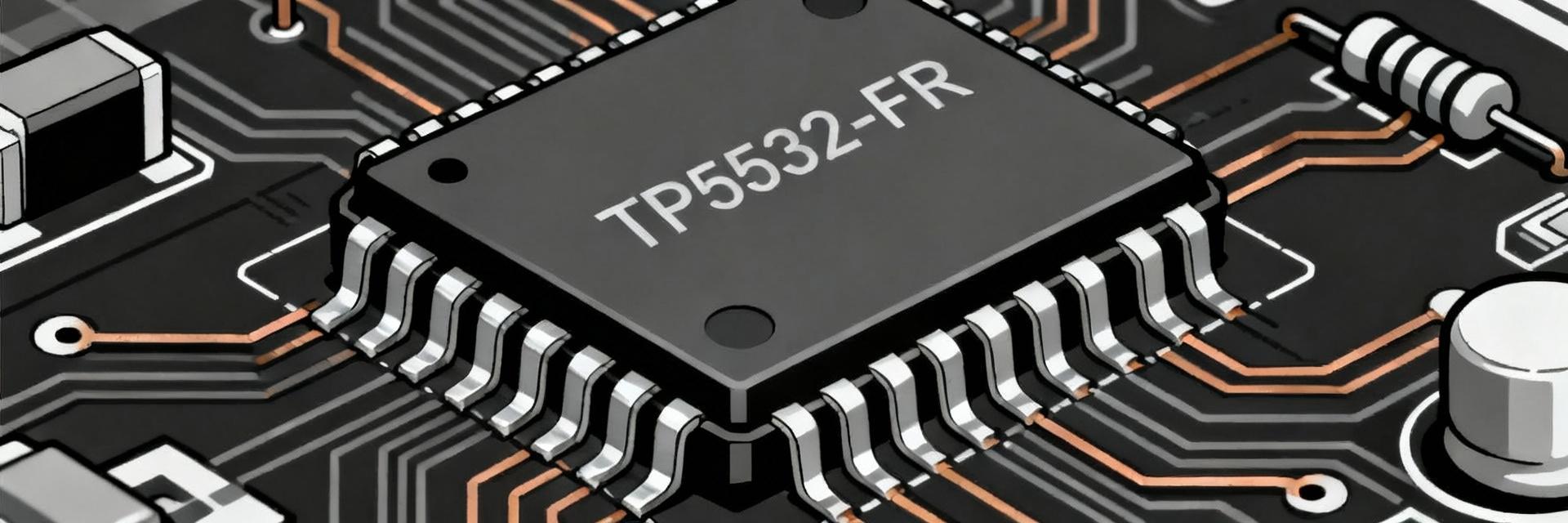
Pinout, Packages & Thermal Considerations (pinout)
Pin function decoding & common pinout diagrams
Point: Correct pin mapping prevents measurement errors and assembly rework. Evidence: Typical pin roles include IN+, IN–, OUT, V+, V–/GND, NC, and an exposed thermal pad. Explanation: Use the exposed pad as the primary thermal and signal ground tie; verify pin numbering across DFN, QFN, and wafer-level packages and follow package-specific recommendations for grounding to minimize offset shifts from ground impedance.
Package thermal behavior and assembly notes
Point: Small packages need careful thermal planning to avoid derating. Evidence: Exposed pad supports heat transfer; junction-to-ambient metrics degrade without thermal vias. Explanation: Implement thermal vias under the pad, follow recommended solder paste patterns, and consider maximum junction temperature in dense boards—adequate thermal vias and copper pour preserve electrical and noise performance under continuous operation.
PCB Footprint & Land Pattern Guidance (footprint)
Recommended footprint dimensions & land pattern details
Point: A correct land pattern ensures solderability and thermal contact. Evidence: For DFN/QFN family, pad geometry balances exposed pad area and signal pads. Explanation: Use manufacturer-recommended pad sizes with modest solder mask clearance and a well-dimensioned exposed pad; common mistakes include over-sized thermal pads that cause solder voids or under-sized pads that reduce thermal dissipation and mechanical reliability.
Stencil, solder paste and assembly tolerances
Point: Stencil design controls paste volume and reflow quality. Evidence: Thermal pad often uses a mid-fraction aperture (e.g., 40–60% of pad area) while signal pads use near-full apertures. Explanation: Apply 0.12–0.15 mm paste thickness typical for fine-pitch reflow; verify with first-article X-ray and AOI; adjust aperture fraction to avoid tombstoning and ensure sufficient wetting of the exposed pad.
Layout, Routing & BOM Integration
Placement & routing best practices for low-noise chopper amplifiers
Point: Layout decisions directly affect offset and low-frequency noise. Evidence: Short input traces, guard rings, and decoupling within 1–2 mm of supply pins preserve published specs. Explanation: Route high-impedance nodes away from digital switching, tie the exposed pad to a single-point ground or star ground as recommended, and place bypass capacitors physically adjacent to supply pins to reduce PSRR-related errors.
Passive selection and BOM notes
Point: Passive choices influence precision and stability. Evidence: Resistor tolerance and capacitor dielectric affect drift and microphonic behavior. Explanation: Prefer metal-film resistors (0.1%–0.01% for critical feedback networks) and C0G/NP0 or stable MLCC dielectrics for filter caps; avoid high-absorption dielectrics on input filters and consider low-noise resistor types in gain networks.
Verification, Testing & Production Checklist
Lab verification to confirm datasheet claims
Point: Reproduce datasheet tests to validate assembled boards. Evidence: Key checks include offset measurement, drift vs. temperature, 0.1–10 Hz noise, PSRR and CMRR. Explanation: Use low-noise sources, guarded fixtures, and proper shielding; set scope/filter bandwidth per datasheet; capture noise in identical bandwidth and units (µVpp) and compare against acceptance tolerances derived from published values.
Pre-production and manufacturing checks
Point: Prevent yield loss by verifying mechanical and process elements early. Evidence: Stencil, land pattern, reflow profile, and exposed pad soldering are frequent failure points. Explanation: Run first-article PCBs through X-ray, AOI, and electrical tests for offset and noise; include assembly notes for exposed pad handling and confirm solder paste volume and reflow thermal ramp to match solder alloy specifications.
Summary
- Use the published offset, drift, noise, Iq, and bandwidth numbers as pass/fail targets—the TP5532-FR acceptance goals should be confirmed on first-article boards with the same supply and load conditions specified in the datasheet.
- Implement recommended land-pattern and a balanced exposed-pad stencil strategy to ensure thermal contact and solder reliability while avoiding voids that can shift electrical behavior.
- Follow layout rules: short input traces, adjacent decoupling (
SEO & publishing notes (quick)
- Primary focus terms to use in metadata: datasheet, footprint, pinout; keep body keyword appearances minimal and natural.
- Suggested meta title: "TP5532-FR Datasheet Deep-Dive — Specs, Pinout & Footprint". Suggested meta description: Practical guide to datasheet specs, pinout decoding, recommended PCB footprint, and layout/test checklist for precision designs.
How should designers validate low-frequency noise from the datasheet?
Measure noise with a low-noise front end and long integration: use a low-drift power supply, guard high-impedance inputs, sample over the 0.1–10 Hz band, and report peak-to-peak using the same filter and averaging method as the datasheet. Shielding and low-noise cabling materially affect results.
What are the most common footprint mistakes to avoid?
Over- or under-sizing the exposed pad, incorrect solder mask clearances, and wrong stencil aperture fractions are frequent issues. Verify pad-to-package alignment, specify correct solder paste thickness, and perform X-ray checks after initial runs to detect voiding or insufficient wetting.
Which bench tests should be prioritized on first-article boards?
Priority tests include DC offset, offset drift across operating temperature swing, low-frequency noise (0.1–10 Hz), output swing into expected loads, and PSRR/CMRR under realistic supply and signal conditions. Use the same measurement bandwidths and load conditions as the datasheet to form acceptance criteria.


