
With a measured unity‑gain bandwidth near 250 MHz and a slew rate around 180 V/µs, the TPH2504-TR is positioned for broader adoption in low‑voltage, high‑speed signal chains in current designs. This report summarizes concise, data‑driven observations, measured performance highlights, and actionable guidance for system integration.
This document covers key specs, recommended test conditions, a compact spec table, measured performance interpretation, benchmarking axes, and practical design recommendations so engineers can validate the part quickly and reliably in their topologies.
1 — Background: what the TPH2504-TR is and typical use cases
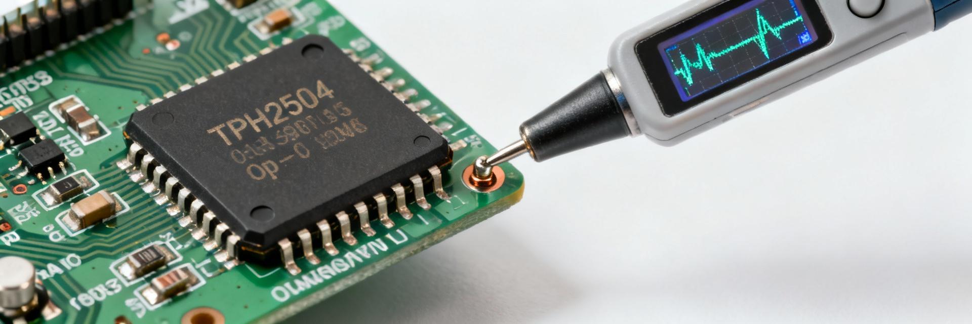
1.1 — Device overview & intended applications
Point: The device is a high‑speed, low‑voltage, rail‑to‑rail I/O operational amplifier aimed at data acquisition front ends, portable instrumentation, and video/sensor interfaces. Evidence: unity‑gain bandwidth ~250 MHz and high slew support fast edges. Explanation: Those attributes make it suitable as a unity buffer, video driver, or front‑end amplifier where speed and low supply operation matter.
1.2 — Key electrical definitions to watch (measurement conditions)
Point: Clear measurement definitions are essential for reproducibility. Evidence: report standard test conditions such as Vsupply (e.g., 5 V nominal), RL, output swing, and 25°C. Explanation: Stating Vsupply, load, and temperature lets teams compare unity‑gain BW, GBP, slew, noise, offset, CMRR, and PSRR under like‑for‑like conditions.
2 — Core specs: tabulated key parameters and what they imply
2.1 — Recommended spec table (what to include)
| Parameter | Typical | Min/Max | Test Conditions |
|---|---|---|---|
| Unity‑gain BW / GBP | ≈250 MHz | — | Vs=5V, RL=1k, 25°C |
| Slew rate | ≈180 V/µs | — | Vs=5V, 100mV→1V step |
| Quiescent current | ~3–5 mA/ch | — | Vs=5V |
| Output drive | ±20–40 mA | — | RL=100–1kΩ |
| Input offset | ~0.5 mV | — | 25°C |
| Input noise (en) | ~6 nV/√Hz | — | 1 kHz |
| CMRR / PSRR | ~70–90 dB | — | 1 kHz, Vs=5V |
| Supply range | ~2.5–5.5 V | — | — |
2.2 — Practical interpretation of each spec
Point: Each spec maps to a design consequence. Evidence: the specs listed above indicate tradeoffs between speed, drive and power. Explanation: For example, ~250 MHz BW dictates keeping closed‑loop gains modest for wide‑band fidelity, while 180 V/µs slew supports sub‑10 ns edges but requires careful layout to avoid ringing and distortion when driving capacitive loads.
3 — Measured performance & data deep‑dive
3.1 — Recommended measurement matrix and representative graphs
Point: A focused measurement matrix yields rapid characterization. Evidence: include small‑signal frequency response (Bode), large‑signal step response, THD+N, output drive vs load, noise density, and offset vs temperature. Explanation: Those figures reveal bandwidth, phase margin, slew‑limited distortion, and thermal drift so designers can validate in‑system performance quickly.
3.2 — Example interpretation of results & tolerance notes
Point: Bench data often differs from datasheet performance due to test setup. Evidence: common sources include fixture bandwidth, probe loading, and supply decoupling. Explanation: Expect modest bandwidth roll‑off and extra peaking if feedback traces are long or decoupling is remote; attribute anomalies to probe compensation, PCB parasitics, or capacitive loads rather than the raw specs.
4 — Benchmarking: comparing TPH2504-TR against peer performance
4.1 — Benchmark criteria and normalized scoring
Point: Use consistent axes for fair comparison. Evidence: compare bandwidth, slew, output drive, quiescent current, noise, supply range, and price‑per‑function. Explanation: Normalize each metric to a 0–1 scale and compute weighted scores or plot a radar chart so teams can quantify tradeoffs instead of relying on single specs.
4.2 — Typical tradeoffs observed (performance vs. power/drive)
Point: High speed often costs power or limits drive. Evidence: devices with >200 MHz BW typically show higher quiescent current and limited heavy‑load swing. Explanation: If primary constraint is battery life choose lower quiescent current parts; if speed dominates accept higher power and implement thermal mitigation and proper decoupling.
5 — Design & test best practices for getting the stated performance
5.1 — PCB layout, decoupling, and stability tips
Point: Layout dictates whether the amplifier meets datasheet behavior. Evidence: short feedback traces, solid ground planes, and 0.1 µF+10 µF decoupling adjacent to supply pins reduce supply impedance. Explanation: For capacitive loads add series isolation (10–50 Ω) or small compensation networks to preserve phase margin and prevent oscillation while maintaining bandwidth.
5.2 — Thermal, reliability and supply sequencing
Point: Continuous high output currents require thermal planning. Evidence: sustained ±20–40 mA outputs increase package temperature and reduce reliability unless PCB copper and thermal vias dissipate heat. Explanation: Include thermal derating in margin analysis and follow controlled supply sequencing to avoid latch‑up; consider series resistors or current limiting during hot‑plug events.
6 — Application examples & engineering recommendations (actionable checklist)
6.1 — Example circuits (recommended configs & typical performance outcomes)
Point: Two compact examples help set expectations. Evidence: (a) unity buffer: closed‑loop BW ≈200–250 MHz, rise time ~1.4 ns; (b) 100 kΩ transimpedance with 1 pF feedback: expected BW ≈30–50 MHz depending on input capacitance. Explanation: These outcomes assume Vs=5V, RL=1k, and disciplined layout to minimize parasitic capacitance.
6.2 — Quick decision checklist for engineers
Point: A short checklist prevents late surprises. Evidence: verify supply range, confirm closed‑loop gain limits, check load/drive needs, validate noise/bandwidth in‑situ, implement layout & decoupling steps, run a thermal check. Explanation: Applying this checklist ensures the TPH2504-TR meets system requirements and that specs and performance are validated in context.
Summary
Concise wrap: The TPH2504-TR combines ~250 MHz bandwidth and ~180 V/µs slew, making it attractive for low‑voltage, high‑speed front ends and buffer roles, provided layout, decoupling, and thermal constraints are addressed. Next steps: execute the recommended measurement matrix, apply the checklist, and benchmark against project constraints before integration.
Key summary
- The TPH2504-TR delivers ~250 MHz unity‑gain BW and ~180 V/µs slew, enabling wide‑band buffering and fast edges when implemented with careful PCB layout and decoupling to realize the stated specs.
- Measure small‑signal BW, large‑signal step, THD+N, and noise density under defined Vsupply and load to confirm real‑world performance and identify fixture‑related deviations early.
- Select this amplifier when speed is primary; if power or heavy output drive dominates, weigh quiescent current and output current limits against system constraints and cooling strategies.
Frequently Asked Questions
What test conditions should I use to measure TPH2504-TR bandwidth and slew?
Use a defined Vsupply (commonly 5 V), RL=1 kΩ, 25°C ambient, and a well‑terminated loop with short feedback traces. For slew rate measure with a 100 mV→1 V or similar large step at the input and capture output edges with a high‑bandwidth scope and properly compensated probe.
How do I avoid instability when driving capacitive loads with this amplifier?
Keep feedback traces short, add a series resistor (10–50 Ω) at the output to isolate capacitive loads, or place a small compensation capacitor in the feedback network. Confirm phase margin on the bench with the intended load and adjust isolation or compensation to suppress peaking or oscillation.
Which specs matter most for choosing the TPH2504-TR in a sensor interface?
Prioritize unity‑gain bandwidth and input noise for wide‑band, low‑level sensor signals, and consider input offset and CMRR for differential sensor outputs. Also validate output drive and quiescent current against system power budget to ensure the part meets both performance and energy constraints.


