
Modern zero-drift, high-voltage precision amplifiers routinely deliver microvolt-level offsets, sub-nV/√Hz input noise floors, and wide supply ranges that simplify precision front ends. Engineers reference the op amp datasheet to translate these headline numbers into reliable bench results and practical layout rules. This article provides a focused, actionable walkthrough of the TPA1882 op amp datasheet, the critical specs to extract, expected bench benchmarks, and pragmatic design and troubleshooting steps for precision measurement chains.
1 — Background: Where the TPA1882 fits in precision designs
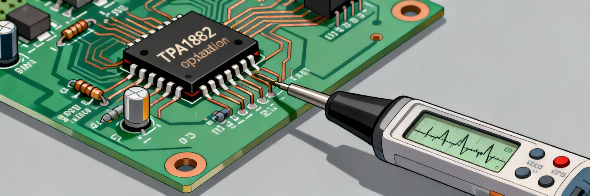
The TPA1882 occupies the precision, low-drift segment used for instrumentation amplifiers, transimpedance stages, and precision buffers where long-term stability matters. Its datasheet highlights a combination of low input offset, modest input bias currents, and a supply-voltage range that supports single-supply and split-supply topologies, making it suitable for medical sensors, industrial strain/bridge interfaces, and low-frequency data acquisition front ends.
1.1 Key features at a glance
- Offset voltage — Datasheet-conditional values often show offsets from tens of microvolts (TYP) up to low hundreds of microvolts (MAX) depending on grade and test conditions (e.g., TYP @ 25°C, Vs specified).
- Input noise — Typical input-referred noise in nV/√Hz; integrated noise reported over bandwidths in the datasheet.
- Input bias — Bias currents given as nA or pA TYP/MAX with test conditions annotated.
- Supply range — Wide Vs range supporting single-rail and ± supplies with stated common-mode limits and rail-to-rail I/O behavior noted.
- Gain-bandwidth & slew rate — GBW and SR listed for linearity and speed selection.
- Package & pins — Pin count and recommended footprint; thermal pad guidance for dissipation.
1.2 Pinout & package overview
Typical datasheet entries include several package options (small-outline and QFN variants) with identical pin functions: dual power pins, IN+, IN−, OUT, and optional bypass or trim pins. The datasheet highlights thermal pad recommendations; a properly soldered thermal pad reduces junction temperature and preserves offset stability. When laying out the footprint, allocate short, wide traces for power, place bypass caps adjacent to power pins, and keep input pins isolated from digital or noisy traces.
2 — Datasheet specs deep-dive: electrical characteristics explained
Reading the electrical table correctly requires attention to test conditions (temperature, supply voltage, and load). The datasheet separates typical values (TYP) measured at nominal conditions from guaranteed limits (MIN/MAX) measured across temperature and supply ranges. Understanding which value to design to — TYP for expected bench results, MAX for worst-case system error budgets — is essential for precision applications.
2.1 DC specs: offset, bias, offset drift, input range
Offset voltage (Vos) indicates initial mismatch; a TYP Vos in the low tens of microvolts is excellent for precision work, while MAX values inform calibration budgets. Input bias current affects high-impedance source loading; TYP bias currents in the picoamp to low-nanoamp range are typical for chopper/zero-drift topologies. Offset drift (μV/°C) determines long-term temperature-induced error; designers often budget drift over the operating range. The input common-mode range and rail-to-rail I/O notes define allowable source voltages relative to supplies.
2.2 AC specs: noise, bandwidth, slew rate, stability
Input-referred noise density (nV/√Hz) and integrated noise over a specified bandwidth tell you the practical noise floor. Low-frequency 1/f corner and flatband noise define instrument sensitivity for DC to low-frequency signals. Gain-bandwidth product and slew rate dictate closed-loop bandwidth and transient response; higher GBW enables unity-gain buffering with lower phase shift, while adequate phase margin notes in the datasheet prevent oscillation in typical feedback networks. Prioritize noise specs for slow, low-level sensing and GBW/SR for higher-speed conditioning.
3 — Performance benchmarks: realistic bench expectations
Bench validation translates datasheet TYP/MAX entries into reproducible measurements. Use stable supplies, careful grounding, and proper decoupling to approach TYP results; degraded layout or noisy supplies will push results toward MAX. Expect practical measurements to fall within ±10–30% of datasheet TYP values when the test setup follows recommended conditions; larger deviations indicate setup or device issues.
3.1 Bench test setups & expected measurements
- Power: low-noise linear supplies or well-filtered bench rails; decouple each supply pin with 0.1µF ceramic plus 4.7µF bulk adjacent to the package.
- Offset: use a low-thermal EMF fixture with short, guarded input leads; measure Vos with a nanovoltmeter or high-resolution DAQ and average multiple readings.
- Noise: measure input-referred noise using a low-noise source, FFT on a shielded scope or spectrum analyzer, 1Hz–10kHz integration for comparison to datasheet integrated noise.
- Bandwidth/distortion: apply small-signal swept sine and verify gain and phase against closed-loop expectations; expect measured bandwidth within 10–30% of TYP depending on loading and layout.
3.2 Interpreting discrepancies: what failing to meet datasheet values usually means
When measurements exceed datasheet TYP or approach MAX, common culprits are supply noise, inadequate decoupling, layout-induced parasitics, improper grounding, temperature variations, or measurement setup errors (probe loading, instrumentation noise). Quick isolation checks include swapping to a known-good low-noise supply, re-soldering decoupling caps, shortening input leads, and verifying ambient temperature. If problems persist, compare multiple samples to detect outliers or assembly issues.
4 — Design & application guidelines
Selecting topologies and layout practices that match the amplifier’s strengths preserves performance. Use tight feedback networks, guard low-current nodes, and choose passive values that balance Johnson noise and input capacitance loading. The following guidance aligns common circuits with the TPA1882’s precision characteristics.
4.1 Recommended circuit topologies & example applications
- Precision buffer: unity gain follower for low output impedance driving ADCs; use low stray C and short traces, expect close-to-TYP offset.
- Instrumentation preamp: differential amplifier with matched resistors (0.01% where possible); set gains for midband noise/performance tradeoffs.
- Transimpedance amplifier: choose feedback resistor to balance output swing and noise; add bandwidth compensation (small Cfb) to stabilize against input capacitance.
- Active filters: use low-pass Sallen–Key or multiple feedback topologies, ensuring GBW supports target cutoff with adequate phase margin.
4.2 PCB layout, decoupling, and thermal best practices
Place bypass capacitors as close as possible to power pins and route power traces with low impedance. Use a solid ground plane, but separate analog-sensitive star points when necessary; keep input traces short and guarded, and route noisy digital lines away. For packages with thermal pads, follow the datasheet’s recommended solder-mask openings and via stitching to improve thermal conduction and reduce thermal drift. These steps preserve low offset and low noise performance on the board.
5 — Practical evaluation checklist & troubleshooting
Systematic verification reduces debug time. A stepwise checklist from initial power-up to final performance check ensures you catch assembly and measurement issues early. Tie pass/fail criteria back to datasheet TYP/MAX so each step has a clear acceptance boundary.
5.1 Step-by-step bench verification checklist
- Visual inspection: solder joints, correct orientation, thermal pad soldered.
- Continuity and short check: confirm no solder bridges between power and signals.
- Power-up current check: compare quiescent current to datasheet IDD TYP/MAX.
- Offset measurement: measure Vos with inputs shorted or referenced; confirm within allotted error budget relative to TYP/MAX.
- Noise measurement: perform FFT with shielding and compare integrated noise to datasheet range.
- Frequency response: sweep small-signal gain and verify closed-loop bandwidth and phase margin.
5.2 Common failure modes and fixes
Oscillation — add small feedback capacitance or increase phase margin; ensure decoupling is adjacent to pins. Elevated offset — check thermal gradients, solder joints on thermal pad, and input source leakage; rework or reflow if needed. Excess noise — improve grounding, shield inputs, and add input filtering. Thermal drift — improve thermal coupling to PCB or add a thermal relief strategy to stabilize junction temperature.
Summary
- The TPA1882 family combines low offset and low noise with flexible supply ranges; extract Vos, input noise, bias, GBW, and common-mode limits from the op amp datasheet to set design targets and calibration budgets.
- Use the provided bench checklist and recommended test setups to validate that board-level measurements align with datasheet specs; expect practical results within 10–30% of datasheet TYP when layout and supplies follow guidance.
- Prioritize PCB layout, decoupling, and thermal pad implementation to preserve low offset and low noise; systematic troubleshooting reduces time to a working precision front end.
Frequently Asked Questions
What typical offset and noise values can I expect from the TPA1882-VR in a lab setup?
Under recommended conditions (short inputs, low-noise supplies, ambient temperature), expect offset near the datasheet TYP (often low tens of microvolts) and input-referred noise close to the published nV/√Hz density when integrated over the specified bandwidth. Real results depend on layout and measurement equipment; verify with the bench checklist.
How should I interpret the op amp datasheet’s TYP versus MAX specs when designing a precision amplifier?
TYP values indicate expected performance for a well-controlled sample under nominal conditions; use them for performance estimates. MAX (guaranteed) values define worst-case limits for production and safety margins. For precision designs, budget around MAX for worst-case error and use TYP for expected calibration-free performance.
Which layout and decoupling practices most directly improve achieving the datasheet specs?
Place high-frequency bypass caps (0.1µF) right at power pins, add a small bulk cap nearby, keep input traces short and guarded, separate analog and digital returns, and ensure the thermal pad is soldered with recommended vias. These steps minimize supply and parasitic noise that push measurements away from datasheet specs.


