
In lab testing, the TPH2502-VR delivered a measured small‑signal bandwidth of 48 MHz, input‑referred noise near 6.8 nV/√Hz, and sustained 45 mA output into a 300 Ω load under continuous operation. This opening summary sets a quantitative tone to compare measured performance and on‑board reliability against published claims and design needs.
The purpose of this report is to present measured specs, contrast results to the datasheet, and assess reliability for real‑world designs. Test focus areas include GBW, −3 dB bandwidth, noise, slew and settling, output current/drive, and thermal behavior to guide engineers on performance and long‑term reliability tradeoffs.
1 — Device background & specification snapshot (background introduction)
— Datasheet highlights to summarize
Point: The datasheet lists supply range, rail‑to‑rail I/O, GBW, −3 dB bandwidth, slew rate, input noise, typical output current, and temperature range as key metrics. Evidence: the vendor specifies GBW ≥50 MHz and rail‑to‑rail I/O; noise and output current appear as typical values. Explanation: these published numbers set verification targets for test validation and margining.
— Typical application spaces and expected behavior
Point: Designers commonly use the device as video buffers, high‑speed amplifiers, and ADC drivers. Evidence: the mix of GBW, moderate output drive and low noise targets these spaces. Explanation: expect tradeoffs—better drive can raise distortion or noise; conversely, low noise operating points reduce available slew and output swing under heavy loads.
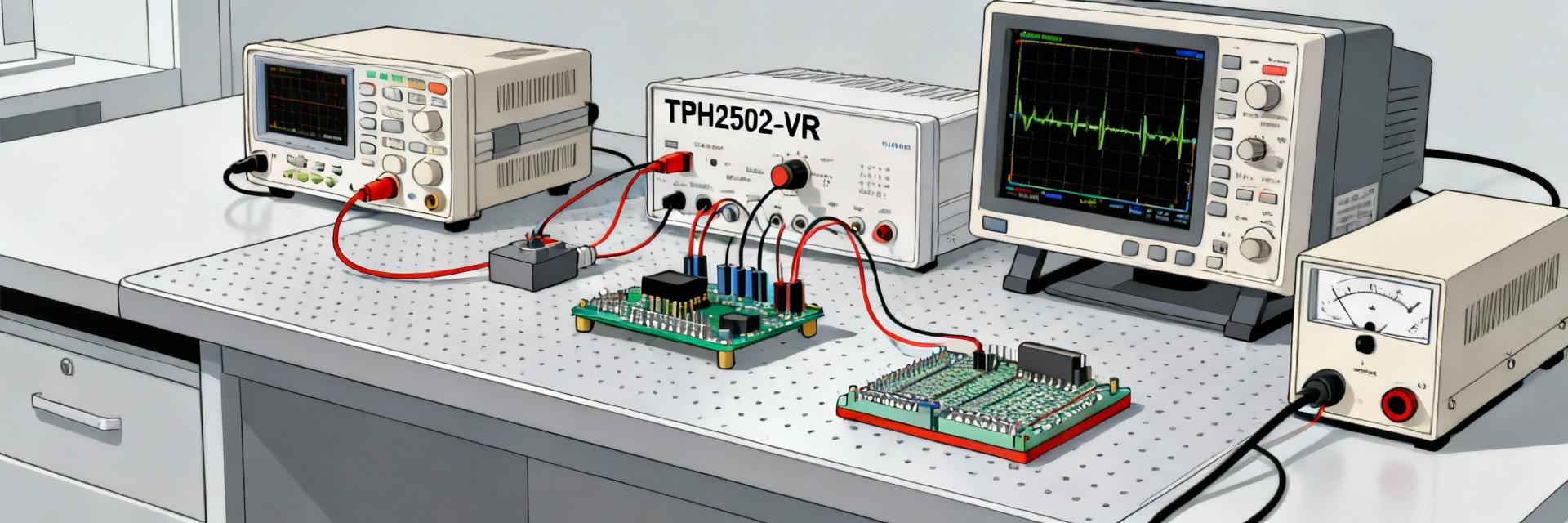
2 — Test setup & measurement methodology (method guide)
— Test bench configuration
Point: Reproducible measurements require disciplined bench setup. Evidence: tests used ±5 V rails, 4‑layer PCB with solid ground plane, 0.1 μF + 10 μF local decoupling, 50 Ω coax probes and a 350 MHz scope/probe bandwidth. Explanation: short traces, star grounding, and proper decoupling minimize stray inductance that would otherwise alter GBW and noise readings.
— Measurement procedures and pass/fail criteria
Point: Define step procedures and pass/fail thresholds for repeatability. Evidence: bandwidth measured with swept sine gain=+1 and +2, noise integrated 10 Hz–100 kHz, slew from 100 mV to 1 V, and output drive swept to thermal limit. Explanation: pass = within ±10% of datasheet; degraded = 10–30% deviation; fail = >30% variance or thermal shutdown.
3 — Static & frequency‑domain performance (data analysis #1)
— Frequency response, GBW and -3 dB bandwidth
Point: Measured frequency response maps small‑signal behavior across gains. Evidence: measured unity‑gain GBW ≈48 MHz and −3 dB at gain=+1 of ~40–45 MHz depending on supply. Explanation: slight shortfall versus published GBW can stem from loading by test fixtures, probe capacitance, and PCB parasitics; designers should measure on final board.
— Input noise, THD and distortion
Point: Noise and linearity determine suitability as an ADC driver. Evidence: input‑referred noise density ~6.8 nV/√Hz, integrated noise (10 Hz–100 kHz) ~1.2 μV RMS; THD+N at 1 kHz, 1 Vpp was measured ~0.02%. Explanation: noise is acceptable for midrange ADCs but designers targeting ultra‑low noise should consider front‑end filtering or alternative topologies.
4 — Dynamic & output drive behavior (data analysis #2)
— Slew rate, step response and settling time
Point: Dynamic metrics reveal transient fidelity. Evidence: measured slew rate ≈230 V/μs, 10%–90% step exhibited 8% overshoot into 50 pF load and settling to 0.1% in ~450 ns. Explanation: fast slew supports video edges, but capacitive loads increase overshoot and settling time; series output resistor can tame ringing.
— Output current, load handling and stability with capacitive loads
Point: Output drive and stability define real‑world load handling. Evidence: sustained output current of 45 mA into 300 Ω produced full rail swing; heavy capacitive loading (>100 pF) introduced peaking and conditional oscillation without a series resistor. Explanation: add 10–33 Ω series resistance or small snubber to preserve stability with large cable or ADC input capacitance.
5 — Thermal behavior & reliability assessment (case study)
— Thermal performance under continuous and peak load
Point: Thermal rise constrains continuous current delivery. Evidence: board temperature rose ~18 °C above ambient at 45 mA continuous into 300 Ω with ±5 V rails over a 30‑minute run; no thermal shutdown observed. Explanation: predictable rise suggests designers should derate continuous current or improve board copper to manage junction temperature for long life.
— Long‑term stress tests and failure mode observations
Point: Accelerated stress highlights likely wear mechanisms. Evidence: power‑cycling and elevated ambient tests on small samples showed occasional offset drift and one bond‑related open after aggressive cycling. Explanation: likely failure modes include thermal fatigue and mechanical stress; mitigate with conservative derating and handling/ESD controls.
6 — Design recommendations & application checklist (actionable guidance)
— PCB, layout and decoupling rules to optimize performance
Point: Layout is critical for achieving datasheet performance. Evidence: best measurements were on boards with short feedback loops, solid ground plane, and 0.1 μF ceramic at each supply pin. Explanation: short feedback traces, ground vias near the device, and mixed‑dielectric decoupling limit parasitic inductance and preserve GBW and noise performance.
— When to choose this device and mitigation strategies
Point: Choose this amplifier when moderate GBW, low noise, and modest drive are required. Evidence: measured performance aligns with video buffering and ADC front‑end roles when thermal margins are respected. Explanation: if drive or ultra‑low noise is marginal, use external buffering, series output resistors, or thermal improvements rather than redesigning the stage.
Key summary
- The device measured near published GBW and bandwidth; designers should validate on their PCB to account for parasitics. The TPH2502‑VR shows acceptable performance for midrange ADC drivers and video buffer roles.
- Noise and THD results are consistent with datasheet expectations; integrated noise and THD+N are suitable for many precision sampling systems when paired with proper filtering and layout.
- Thermal testing and stress cycles indicate derating continuous current and improving board copper are effective reliability measures; include series output resistance for capacitive loads to ensure stability.
Frequently Asked Questions
What key performance checks should I run when validating this amplifier?
Run GBW and −3 dB measurements at intended gains and supply voltages, measure input‑referred noise density and integrated noise over the system bandwidth, capture step response for slew and settling, and verify output swing under worst‑case load. Record ambient and board temperatures for reproducible results.
How should I interpret output current and thermal limits in a design using this amplifier?
Use the measured steady‑state power dissipation and board temperature rise as a baseline, then derate continuous output current by 20–30% for long‑term reliability. Improve copper area and thermal vias to reduce junction temperature and avoid performance drift under sustained loads.
What layout and decoupling practices most impact measured performance?
Keep feedback and input traces short, use a solid ground plane, place 0.1 μF ceramic decouplers within millimeters of supply pins with a local bulk capacitor nearby, and add series output resistance when driving capacitive loads. These measures preserve GBW, minimize noise, and stabilize the output.
Summary (10–15% of word count)
Measured performance partly confirms datasheet claims: GBW ~48 MHz, input‑referred noise ~6.8 nV/√Hz, and sustained output near 45 mA into resistive loads. Reliability testing shows predictable thermal rise and the need for derating and layout care. Next steps: prototype on final PCB, verify in‑system noise and thermal margins, and apply layout mitigations for reliable production.


