
Designers commonly screen op amps by a short list of measurable attributes — supply current, input offset, GBW, and output swing — to decide fit quickly. This note summarizes the TPA6581-SC5R with a compact, testable spec checklist and practical measurement guidance so engineers can evaluate fit without wading through full datasheets.
(1/5) Quick product snapshot & identifiers — background
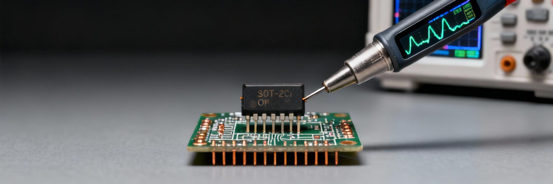
Part code, package & marking
Point: Identify the exact ordering code and package variant before board placement. Evidence: The full part name is TPA6581-SC5R and variants exist with different tape/reel and package suffixes; common board markings use the short part code and a lot code. Explanation: Confirm package type (SOT-23/SC or equivalent), pin count and thermal pad presence on your BOM and silkscreen to avoid assembly mismatches.
Operating ranges & primary use cases
Point: Know the rated operating window and target applications to screen quickly. Evidence: The device is specified for low-voltage single-supply operation with a limited recommended Vs window and defined absolute maximums in the datasheet; typical domains are sensor front ends and low-voltage battery systems. Explanation: Use the datasheet tables for exact temperature and supply limits, and pre-filter candidates based on whether your system runs near the rails or requires extended temperature ranges.
(2/5) Absolute & recommended electrical specs — data analysis
Power & supply characteristics
Point: Power budget and supply behavior are first-order selection criteria in portable designs. Evidence: Datasheet op amp specs list recommended Vs range, quiescent current (Iq) per amplifier, and absolute maximum supply; some low-voltage CMOS parts include supply sequencing or reverse-voltage cautions. Explanation: Match Iq to battery budget, verify that recommended Vs covers your worst-case drop, and note any sequencing or capacitor-on-rail notes that affect system power-up behavior.
Input/output DC characteristics
Point: DC accuracy and output compliance determine front-end performance. Evidence: The datasheet provides input offset (typical and max), input bias currents, input common-mode range, and output swing to rails under specified loads and temperatures. Explanation: Always compare those numbers under your intended conditions (Ta, RL, Vs) — for rail-to-rail I/O parts, confirm the specified load (kΩ or mA) where output swing is measured to avoid surprise clipping in application.
(3/5) Key performance metrics & benchmark guidance — data analysis
AC behaviour (GBW, slew rate, stability)
Point: Frequency response and stability set closed-loop bandwidth and transient fidelity. Evidence: The datasheet lists gain-bandwidth product, slew rate, and often phase margin or stability recommendations for common gains — these performance metrics determine achievable closed-loop bandwidth and margin. Explanation: Use unity-gain and typical-gain test circuits to reproduce GBW and slew, and ensure your chosen feedback network yields adequate phase margin for the required gain and capacitive loading.
Noise, distortion & dynamic accuracy
Point: Dynamic accuracy matters for sensor preamps and precision filters. Evidence: Input-referred noise density, THD or output distortion figures, and settling time are given under defined test conditions (gain, source impedance, RL). Explanation: Benchmark under comparable source impedance and load; for low-voltage RRIO CMOS op amps expect modest noise and THD suited to many sensors but verify settling time when driving ADC inputs at your required resolution and throughput.
(4/5) Measurement & PCB design recommendations — method guide
Recommended test circuits & conditions
Point: Reproducible test setups are essential to match published numbers. Evidence: Typical datasheet measurements use unity-gain or defined closed-loop gain (for example, gain = 1 and gain = 10), specified RL, supply voltage, and ambient temperature. Explanation: Replicate those conditions: use low-inductance supply decoupling, 0.1 μF plus 10 μF near the device, a low-noise signal source, and scope probes with proper grounding to avoid injecting measurement artifacts into small-signal noise and GBW tests.
PCB layout, decoupling & thermal considerations
Point: Layout and thermal limits affect continuous operation and noise performance. Evidence: Datasheet and package thermal resistance figures show how ambient temperature and copper area change allowable dissipation; layout guidance calls for close decoupling and short ground returns for low-noise paths. Explanation: Place bypass caps within 1–2 mm of V+ and ground pins, use a solid ground plane, guard sensitive inputs, and provide copper keepouts or thermal vias to reduce junction temperature under sustained loads.
(5/5) Application fit, trade-offs & quick selection checklist — action
Typical application examples & decision criteria
Point: Map device strengths to concrete use cases to accelerate selection. Evidence: The part targets low-voltage, low-power applications such as portable sensor preamps, active single-supply filters, and general-purpose buffers where moderate GBW and rail-to-rail I/O are sufficient. Explanation: If your design needs high-voltage rails, sub-μV offset, or very wide GBW, consider alternatives; for battery-powered sensors, prioritize Iq, input offset, and output swing under expected RL.
Quick selection checklist & design trade-offs
Point: A short checklist speeds go/no-go decisions on the bench. Evidence: Key items are supply compatibility, Iq, noise budget, GBW for target closed-loop gain, output swing under load, and package/temperature constraints. Explanation: Trade-offs are typical: lower power reduces bandwidth and increases offset drift; higher GBW increases quiescent current. Use this checklist during initial screening, then bench-verify the top candidates.
Summary
Concise recap: This note aimed to give a compact, testable spec summary so engineers can quickly judge whether the TPA6581-SC5R fits their design by focusing on supply behavior, DC accuracy, GBW/slew, and output swing. Verify final numbers against the official datasheet and run bench tests under your actual load and ambient conditions to confirm fit and margin for your application.
(Key summary)
- Supply & power: Confirm recommended Vs and quiescent current vs battery budget; watch absolute maximums and any sequencing notes before layout and BOM freeze.
- DC accuracy: Check input offset and bias under your operating temperature and source impedance to ensure margin for calibration or trimming.
- AC and dynamic: Match GBW and slew to closed-loop bandwidth and settling requirements; test with your gain and load to reproduce datasheet behavior.
- Layout & thermal: Use close decoupling, solid ground, guarding for low-noise paths, and adequate copper for thermal dissipation to keep performance predictable.
(Common questions)
How do I verify TPA6581-SC5R input offset in my circuit?
Measure offset by configuring the amplifier in unity gain with inputs shorted through a small resistor to avoid oscillation; record Vout at nominal Vs and temperature, then compute input-referred offset using the closed-loop gain. Repeat across temperature to estimate drift and compare with datasheet max values.
What test conditions reproduce TPA6581-SC5R GBW and slew rate?
Use unity-gain buffer and a noninverting gain of 10 to measure gain-bandwidth and slew. Drive with a low-impedance source, monitor the output with a low-capacitance probe, and ensure supply decoupling matches datasheet recommendations; measure at specified Vs and Ta to match published performance metrics.
What PCB layout steps reduce noise for TPA6581-SC5R applications?
Place bypass caps adjacent to supply pins, route ground to a solid plane, minimize loop area for input and feedback traces, and use guarded traces for high-impedance nodes. These steps reduce injected noise and help the device meet its datasheet noise and stability specifications in real systems.


