
The TPA1286 family lets designers set any gain from 1 to 1,000 with a single external resistor — a capability that drives its adoption in precision sensing applications. This article provides an actionable, datasheet-focused analysis of CMRR and gain behavior for designers working with TPA1286U-VS1R, plus practical measurement steps and design guidance to validate real-world performance.
Product background & key datasheet highlights
What the TPA1286U-VS1R is and where it\u2019s used
The TPA1286U-VS1R is a zero-drift instrumentation amplifier with single-resistor gain setting (gain range 1\u20131000), rail-to-rail output capability, and low input bias current suitable for precision bridge and low-frequency sensor front ends. Its architecture targets low offset drift and long-term stability, making it useful for strain gauges, thermistor bridges, and other small-differential-signal sensors that coexist with large common-mode voltages.
Key electrical specs to pull from the datasheet (what to extract)
When extracting datasheet numbers, capture typical and worst-case values and the measurement conditions (supply, temperature). Pull offset, bias current, supply current, slew rate, common-mode range, output swing, and recommended Rg range. Below is a compact reference table for quick comparison; verify exact limits and conditions in the official datasheet for production decisions.
| Spec | Typical | Max | Unit |
|---|---|---|---|
| Input offset voltage | ~25 | 100 | µV |
| Input bias current | 10 | nA | |
| Supply current | ~2.5 | 4 | mA |
| Slew rate | 1 | 5 | V/µs |
| Common-mode input range | Rail ±0.1 | — | V |
| Output swing | Rail ±20 | — | mV |
| Recommended Rg range | 100 | 100k | Ω |
CMRR fundamentals for instrumentation amplifiers (data analysis)
What CMRR means in practical terms for TPA1286 applications
CMRR quantifies rejection of common-mode signals and is expressed in dB: CMRR(dB) = 20·log10(Ad/Ac), where Ad is differential gain and Ac is common-mode gain. High CMRR ensures a small differential input (microvolts to millivolts) is not overwhelmed by large common-mode voltages from sensor offsets or EMI. For sensor accuracy, translate CMRR into an equivalent input error at expected common-mode levels to set design margins.
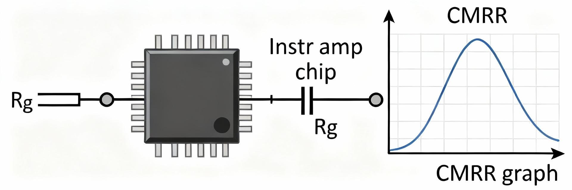
Typical CMRR behavior vs gain (how to read the datasheet graphs)
Datasheets typically show DC CMRR and CMRR vs frequency. Expect the highest CMRR at DC with gradual degradation at higher frequency — the −3 dB point indicates where rejection falls notably. For the TPA1286 family, extract DC CMRR and the frequency at which CMRR drops by 3\u20135 dB; annotate curves at the gains you plan to use to verify acceptance across your signal band.
Gain setting: resistor calculation and practical effects (method guide)
How to calculate Rg for target gain (step-by-step)
The datasheet gives a single-resistor formula of the form Gain = 1 + K/Rg, where K is an internal constant specified therein. Algebraically, Rg = K / (Gain - 1). Using a common example constant K = 100kΩ for worked examples (verify K in the datasheet):
| Target gain | Example Rg (K=100kΩ) | Expected impact |
|---|---|---|
| 1 | Open (∞) | Max bandwidth, lowest noise contribution |
| 10 | 11.1kΩ | Moderate BW reduction, improved signal amplitude |
| 100 | 1.01kΩ | Reduced BW, higher input-referred noise |
| 1000 | 100Ω | Significant BW limit, layout-sensitive CMRR |
Choose precision Rg (0.1\u20131% depending on accuracy needs). Lower Rg values increase current and can introduce resistor noise; balance tolerance vs noise when specifying part values.
How gain choice affects bandwidth, noise, and CMRR
Higher gain typically reduces closed-loop bandwidth and can increase input-referred noise after scaling; CMRR can become more sensitive to mismatch and layout at very high gains. Consult gain-dependent curves in the datasheet (noise vs gain, bandwidth vs gain) and follow layout practices: short, matched input traces, star grounding, and local decoupling to preserve both CMRR and noise performance.
Measurement & validation: bench procedure to verify CMRR and gain (method guide / data analysis)
Recommended lab setup and instruments
A robust setup includes: precision function generator(s) or differential source, low-noise differential amplifier or buffer for stimulus, calibrated precision Rg resistors, high-resolution oscilloscope with differential probe, spectrum analyzer or FFT-capable DAQ, and a stable power supply. Use shielded connections and a driven guard if measuring microvolt-level offsets to avoid probe loading and leakage.
Step-by-step measurement procedure and data analysis
Step 1: Configure the amplifier with the chosen Rg and apply a small differential input (e.g., 1 mVpp); measure output amplitude to compute Ad = Vout/Vin. Step 2: Apply a known common-mode voltage (Vc) with zero differential input; measure Vout to compute Ac = Vout/Vc, then CMRR(dB)=20·log10(Ad/Ac). Step 3: Repeat across frequency to produce CMRR vs frequency. Watch for probe loading, ground loops, and source imbalance; mitigate with buffering and symmetry. Compare measured curves to datasheet typical/min specs to accept or iterate design changes.
Application examples & design checklist (case study + action recommendations)
Two short application vignettes (one low-frequency sensor, one higher-frequency front end)
Low-frequency: bridge strain gauge. Choose moderate gain (10\u2013100) to bring microvolt-level bridge signals into ADC range, prioritize DC CMRR and thermal stability, use low-drift precision Rg, and enforce symmetrical routing. High-frequency: vibrational sensor or biopotential frontend. Favor lower gain at the amplifier stage and use subsequent filtering/amplification to meet bandwidth; verify CMRR across the instrument bandwidth and control input protection to prevent slew-rate issues.
Practical design checklist before production
- Verify Rg value and tolerance against datasheet formula and expected gain; confirm K constant from the datasheet.
- Simulate CMRR with expected common-mode amplitudes and frequency content; plan margins for EMC events.
- Specify input protection and filtering that do not unbalance the inputs; match source impedances.
- PCB layout: matched differential traces, local decoupling, single-point star ground, minimize input trace length.
- Thermal and supply decoupling: verify performance across anticipated operating temperature and supply variations.
Summary
The TPA1286U-VS1R delivers flexible single-resistor gain and low-drift performance ideal for precision sensors; designers must read CMRR curves and gain-dependent specs to predict real-world behavior. Follow the calculation steps for Rg, validate gain and CMRR on the bench, and apply the layout checklist to preserve performance before committing to a PCB spin. Download the TPA1286 datasheet and run the provided bench checklist before committing to a PCB spin.
- Single-resistor gain simplifies configuration, but verify Rg and its noise/tolerance impact against expected bandwidth and CMRR.
- Measure CMRR by computing Ad and Ac across frequency; mitigate probe loading and source imbalance for credible results.
- High gain narrows bandwidth and increases layout sensitivity; prioritize matched routing and local decoupling to protect CMRR.


