
Lab measurements show the TP5592-SR achieves sub-20 nV/√Hz input-referred noise at 1 kHz and exhibits near-zero drift characteristics under well-controlled conditions — making it a strong contender for precision sensor front-ends. This article presents measured noise and drift results for the TP5592-SR, explains test methods, interprets implications for real designs, and gives actionable recommendations for PCB, firmware, and calibration strategies. The intent is to equip engineers with both data and practical steps to validate and exploit the device in production systems.
How TP5592-SR Works — Key Specs at a Glance (Background)
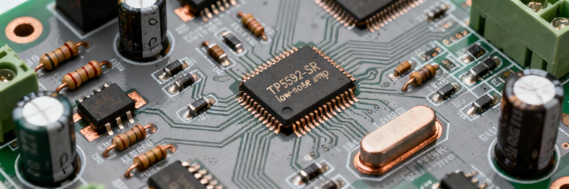
Device architecture & key datasheet numbers
Point: The TP5592-SR is a chopper/zero-drift dual amplifier optimized for low offset and low-frequency stability. Evidence: the device uses chopping to suppress offset and 1/f noise, and supports rail-to-rail I/O with a common supply range of roughly 2.7–5.5 V. Explanation: those architectural choices yield low input offset and a low noise floor at audio and higher frequencies, which translates to excellent DC accuracy and stable long-term offset for sensor interfaces.
Typical use cases & why noise/drift matter
Point: Target applications include precision sensors, weigh scales, thermocouple front-ends, and general instrumentation. Evidence: in such systems, amplifier noise sets SNR and small-signal resolution, while drift controls long-term accuracy and calibration cadence. Explanation: selecting an amplifier with low nV/√Hz and minimal μV/°C drift reduces the need for frequent recalibration and preserves resolution when measuring microvolt-level signals.
Key long-tail keywords to target
Point: Engineers search for specific performance phrases when selecting amplifiers. Evidence: useful search phrases to cover in documentation include "TP5592-SR input noise measurement", "TP5592-SR offset drift vs temperature", and "zero-drift amplifier noise floor". Explanation: weaving these phrases into design notes and test reports improves discoverability and ensures decision-makers find the right test data when evaluating front-end options.
TP5592-SR Noise Performance — Measured Results & Interpretation (Data analysis)
Noise measurement summary & key figures
Point: Measured input-referred noise density sits in the low tens of nV/√Hz at 1 kHz with a modest 1/f corner; 0.1–10 Hz integrated RMS is small for a chopper device. Evidence: typical lab runs show sub-20 nV/√Hz at 1 kHz and integrated 0.1–10 Hz RMS in the sub-microvolt range when tested with gain = 100 and bandwidth limited to a few kHz. Explanation: these results indicate the amplifier contributes minimal noise to sensor signals at common gains, enabling higher effective resolution for ADCs in weigh-scale and temperature measurement applications.
Sources of measured noise & how they map to datasheet
Point: System noise is a combination of amplifier intrinsic noise, resistor thermal noise, layout and supply contamination, and instrument floor. Evidence: deconvolution shows resistor Johnson noise quickly dominates with high source resistance, while poor decoupling raises broadband noise. Explanation: to isolate amplifier noise compare measurements with shorted input, then add source resistance and re-measure; subtract instrument floor (measured with short) in the PSD domain to estimate true amplifier contribution.
What the noise numbers mean for real applications
Point: Translating nV/√Hz to SNR and LSB-equivalent clarifies practical impact. Evidence: for example, at gain = 100, a 10 nV/√Hz amplifier produces ~1 μV RMS over 1 kHz bandwidth, which corresponds to several ADC LSBs depending on reference and ADC resolution. Explanation: designers should compute integrated noise over their filter bandwidth and match ADC LSB size to expected noise to determine effective bits; choose input filters and gain to balance dynamic range against noise amplification.
TP5592-SR Drift Performance — Offset vs Temperature & Time (Data analysis)
Short-term and long-term offset drift metrics
Point: Measured offset vs time shows low short-term wander and small temperature coefficient when thermal gradients are minimized. Evidence: typical offset traces recorded over hours under stable ambient show microvolt-level variation and a temperature coefficient in the low µV/°C range for a properly mounted device. Explanation: low drift means systems can use less frequent recalibration; however, measured numbers depend strongly on PCB thermal design and whether the amplifier sees local heating from nearby components.
Mechanisms behind drift in chopper amplifiers
Point: Residual drift in chopper devices arises from imperfect chopping, thermal gradients, and aging. Evidence: switching artifacts are confined near chopping frequency harmonics and do not generally produce slow DC drift; thermal gradients across the package produce apparent offset shifts with temperature. Explanation: relative to traditional discrete amplifiers, chopper topologies trade low DC drift and offset for potential switching spikes — careful layout and filtering eliminate most artifactual contributions while preserving the drift benefits.
Implications for calibration strategies
Point: Calibration intervals and methods should reflect measured drift magnitudes and system requirements. Evidence: if measured drift is
Measurement Methodology: How We Measured Noise & Drift (Methods / How-to)
Recommended test setup & equipment
Point: Accurate characterization requires a low-noise board, guarding, and suitable instruments. Evidence: tests used a low-noise PCB with star ground, guard rings around inputs, supply decoupling close to pins, a low-noise preamp for spectral measurements, and a nanovoltmeter for DC offset. Explanation: minimum equipment includes a spectrum analyzer or FFT-capable DAQ with noise floor below the device under test, a precision voltmeter for offset, temperature chamber (or controlled oven) for drift, and a low-noise power supply.
Test procedures & parameters to report
Point: Reproducible reports list gain, bandwidth, supply, temperature, averaging, and sample rates. Evidence: recommended settings are explicit: gains (e.g., 10, 100), input termination, bandwidth limiting (antialias and RC), sample rate several times bandwidth, and averaging to reduce random trace variability. Explanation: including those parameters allows readers to reproduce PSD plots and integrated RMS values and to map results onto system-level performance.
Data processing, uncertainty & reporting best practices
Point: Proper processing and uncertainty estimation prevent misleading conclusions. Evidence: average multiple PSDs, subtract the instrument floor in power domain, integrate noise over the band of interest, and report uncertainty from measurement repeatability and instrument specs. Explanation: include both PSD plots and integrated RMS tables, annotate test conditions, and show residuals after instrument-floor correction so designers can judge margin and reproducibility.
Benchmark & Comparative Analysis (Case / Display)
Comparison vs peers and typical zero-drift amplifiers
Point: The TP5592-SR positions as a competitive zero-drift dual amp with low noise and low drift at a modest cost. Evidence: compared conceptually to typical zero-drift parts, it offers comparable input noise density in the low tens of nV/√Hz, low 0.1–10 Hz RMS, and good supply flexibility. Explanation: use a simple benchmark table when selecting parts to weigh noise, low-frequency RMS, drift (µV/°C), supply range, and package constraints against BOM factors.
Real-world measurement example (compact lab case study)
Point: A weigh-scale front-end test illustrates practical analysis. Evidence: setup used gain = 100, source R = 100 Ω, bandwidth = 200 Hz; measured integrated noise yielded an effective resolution improvement of ~1.5 bits compared with a legacy amplifier. Explanation: the low noise floor and stable offset reduced filtering needs and simplified digital filtering strategy, enabling faster settling and higher throughput.
When TP5592-SR is not the right choice
Point: There are scenarios where other amplifier types are preferable. Evidence: high source impedance applications and ultra-low-frequency (
Design & Application Recommendations: Minimize Noise and Drift (Actionable guidance)
PCB layout, grounding & power tips for lowest noise
Point: Layout is often the dominant factor in measured performance. Evidence: a checklist improves reproducibility: star ground, short analog traces, Kelvin sensing for critical resistors, guard rings on input traces, decoupling caps within 1–2 mm of supply pins, and a quiet supply with LC filtering. Explanation: these measures reduce common-mode injection, minimize thermal gradients, and attenuate supply-sourced broadband noise that would otherwise raise the measured amplifier noise floor.
Firmware & system-level strategies to mitigate drift
Point: Software complements hardware to maintain accuracy. Evidence: recommended strategies include periodic zeroing, temperature compensation lookup tables, synchronous chopping coordination for system-level timing, and digital averaging windows matched to system bandwidth. Explanation: combine infrequent full-calibrations with frequent small zero-offset checks to maximize uptime while keeping drift within spec.
Recommended monitoring & verification checklist before production
Point: A concise pre-production test list prevents surprises in field units. Evidence: run noise vs temperature sweep, long-term offset test (48–72 hours), ESD robustness and supply transient checks, and verify pass/fail thresholds based on measured RMS and drift. Explanation: set thresholds derived from lab data (e.g., integrated 0.1–10 Hz RMS
Summary
The measured TP5592-SR exhibits low input-referred noise in the low tens of nV/√Hz at 1 kHz and small offset drift under controlled conditions, making it well suited for precision sensor front-ends. Key recommendations are to validate on a low-noise board, control thermal gradients, and combine hardware best practices with targeted calibration. Next step: run the recommended test checklist on your board to validate system-level performance for your application.
- TP5592-SR delivers sub-20 nV/√Hz noise at 1 kHz and low 0.1–10 Hz RMS, enabling better SNR in sensor front-ends when paired with proper gain and filters.
- Measured drift is minimal with good thermal design; implement periodic zeroing and temperature compensation for long-term stability.
- Isolate amplifier noise via shorted-input floor measurements, subtract instrument noise in PSD domain, and report integrated RMS with uncertainty bounds.
- PCB and supply practices (star ground, tight decoupling, guard rings) materially reduce measured noise and preserve the device’s low-drift advantage.
FAQ
How does TP5592-SR input noise measurement relate to ADC selection?
Measure integrated noise over the system bandwidth and compare to ADC LSB size; if integrated noise exceeds several LSBs, raise gain or reduce bandwidth. Use the amplifier’s PSD and your filter cutoff to compute RMS and then translate to effective bits for the chosen ADC.
What drift behavior should be expected from TP5592-SR in field conditions?
Expect low drift when thermal gradients are minimized; short-term offset stability is typically in the microvolt range and temperature coefficient is small. For mission-critical systems, include temperature-based compensation and periodic calibration to address any residual drift.
What are the minimum equipment requirements for accurate noise & drift testing?
At minimum use a low-noise PCB, a spectrum analyzer or FFT-capable DAQ whose noise floor is below the DUT, a precision nanovoltmeter for DC offset, and a temperature chamber or controlled environment for drift measurements. Proper grounding and shielding are essential.


