
Rated for operation up to 105°C and supporting a wide supply range (typ. 1.3–5.5 V), the S-35190AH-T8T2U targets automotive and industrial real-time clock needs that demand ultra-low standby current and robust backup switching. This article condenses the S-35190AH-T8T2U datasheet into the essential specifications, measured behavior, and practical validation guidance so designers can quickly assess fit and plan testing. Point: the device’s temperature rating and supply flexibility position it for harsh environments. Evidence: the official RTC datasheet enumerates the 1.3–5.5 V range and high-temperature spec. Explanation: that combination reduces external regulator needs in multi-voltage systems and simplifies backup arrangements for battery-backed clocks.
Goals for the reader are practical: summarize core specs in a compact table, explain how to read and interpret the datasheet tables and graphs, and provide clear integration tips plus a bench validation checklist. Point: designers need not only numbers but interpretation and test procedures. Evidence: the datasheet supplies raw tables and timing diagrams; this article translates those items into stepwise checks and expected pass/fail thresholds. Explanation: following these steps reduces iteration in hardware bring-up and ensures reliable timekeeping across supply transitions and temperature extremes.
1 — Product Overview & Key Specifications (background)
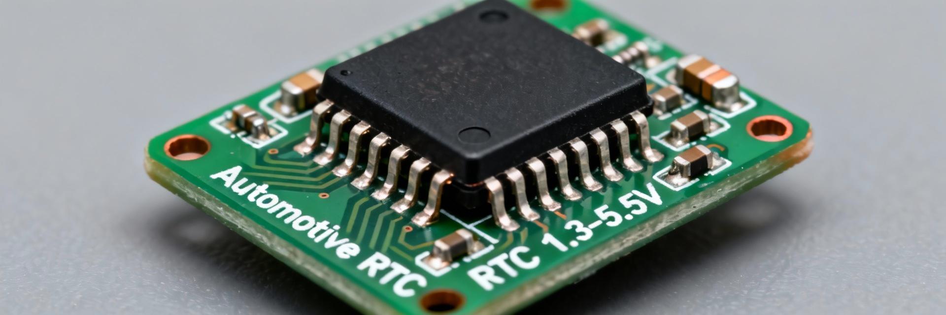
Part number, variants and target applications
Point: S-35190AH-T8T2U is a member of the S-35190A H-series of real-time clock ICs with automotive-oriented temperature and qualification variants. Evidence: the part-number suffixes (H, package code) indicate high-temperature/automotive grade and package type; ABLIC’s family includes related variants tuned for different packages and feature sets. Explanation: designers choose the T8T2U suffix to get the 8-pin TSSOP package with the H-series temperature/qualification, making it suitable for battery-backed clocks, instrument clusters, telematics modules, data loggers, and industrial controllers that require ultra-low backup drain and package compatibility with standard PCB footprints.
Core electrical specs at a glance
Point: key electrical boundaries to validate early are supply range, operating temperature, package, and idle/active/backup currents. Evidence: the datasheet lists nominal supply 1.3–5.5 V, operating range –40°C to 105°C, package: 8‑TSSOP, and separate current figures for run, standby, and battery-backed modes. Explanation: these numbers dictate regulator choices, expected battery life, and thermal design; use the quick table below as the first pass during part selection and BOM review.
| Parameter | Typical / Note |
|---|---|
| Supply voltage (VDD) | 1.3 – 5.5 V (operational range) |
| Operating temperature | –40°C to +105°C (automotive H-grade) |
| Package | 8‑pin TSSOP |
| Typical active current | sub‑µA range (see datasheet ICC run/active) |
| Backup current (VBAT mode) | ultra‑low standby/backup (datasheet typical value) |
| Interface | 3‑wire serial (serial data, clock, chip enable) |
Feature highlights and competitive positioning
Point: the device’s defining features are ultra-low backup current, integrated calendar/alarm, and a compact, automotive-capable package. Evidence: the datasheet calls out a 3‑wire serial interface, automatic backup switching, on-chip calendar with alarm, and oscillation support for 32.768 kHz crystals. Explanation: these map directly to common design requirements—minimizing coin‑cell drain, simple MCU interface, reliable alarm generation for wake events, and robust operation across wide temperatures—making the S-35190AH-T8T2U competitive for low‑power vehicle modules and long-life industrial sensors.
2 — Electrical Characteristics & Performance Data (data analysis)
Voltage, current and timing limits — how to read the tables
Point: datasheet tables provide min/typ/max columns and separate rows for conditions; interpreting them correctly is essential to margin budgeting. Evidence: the electrical characteristics section lists VIN min/max, ICC in run/standby/backup, and timing/capacitance constraints with qualification conditions (e.g., TA = –40°C to +105°C, VDD levels). Explanation: treat “typical” values as design guidance, not guaranteed; size power budget from the “max” (or guaranteed) columns plus derating at temperature extremes. For backup budgeting, use the VBAT-mode ICC figure at the worst-case temperature to compute battery lifetime and margin for leakage growth over time.
Timekeeping accuracy & oscillator behavior
Point: frequency tolerance and temperature drift determine long-term timekeeping error—critical for interval timing and timestamping. Evidence: the datasheet presents oscillator frequency tolerance (initial ±ppm) and temperature dependency curves (error vs. °C), often with separate plots for typical drift. Explanation: use the datasheet’s ppm numbers and drift curves to derive expected seconds-per-day error across your operating range; for precision applications, apply temperature compensation or external timing discipline. If the datasheet provides plots, extract worst‑case ppm at the system’s temperature extremes to set acceptance thresholds in thermal-vs-timekeeping tests.
Alarm, interrupt and calendar function specs
Point: alarm resolution, debounce, and interrupt latency affect how the system responds to time-based wake events. Evidence: timing diagrams and functional tables in the datasheet define alarm match conditions (seconds/minutes/hours/day), interrupt behavior (edge/level), and any internal debounce intervals or command execution latencies. Explanation: validate that alarm resolution meets the application (e.g., 1‑second resolution), and ensure MCU ISR handling accommodates the documented latency. For critical wake events, include margin testing of alarm-to-MCU-wakeup path and verify behavior across supply transitions using the datasheet timing numbers as pass/fail criteria.
3 — Interface, Pinout & Package Details (method/guideline)
3-wire serial protocol: signals, timing and command flow
Point: the S-35190AH-T8T2U uses a compact 3‑wire serial protocol that is similar to, but distinct from, SPI and I²C. Evidence: the interface section of the datasheet documents three signals (chip enable, serial clock, serial I/O) and provides timing diagrams for setup/hold times, clock high/low durations, and command framing. Explanation: implement the host-side driver to respect the datasheet’s timing margins, use the recommended command sequence for register reads/writes, and include retries when crossing power domains. For example, assert chip‑enable, shift address/command bits on clock edges, and sample data per the specified timing to avoid misreads during fast MCU clocking.
Pin functions and recommended PCB footprint
Point: correct pin assignment and footprint reduce rework and thermal issues. Evidence: the package drawing and pin table show VDD, VBAT, GND, SCLK, SI/SO or IO, and NC pins along with recommended land pattern dimensions for the 8‑TSSOP. Explanation: follow the recommended land pattern, place decoupling capacitor close to VDD pin, route VBAT trace short and low-impedance, and keep the 32.768 kHz crystal and its load capacitors adjacent to the oscillator pins to minimize stray capacitance. If the datasheet includes a thermal pad note, respect solder mask openings and keep copper pour for thermal dissipation where recommended.
ESD, packaging and handling notes
Point: ESD and moisture sensitivity affect handling and assembly yield. Evidence: the datasheet typically lists ESD robustness (HBM/MM) and moisture sensitivity level along with recommended storage/handling precautions. Explanation: align PCB assembly ESD controls to the datasheet class, follow bake and moisture control procedures if the part has MSL listing, and avoid mechanical stress on leads during reflow. For automotive-grade parts, confirm incoming inspection and reel handling per supplier recommendations to preserve reliability.
4 — Power Backup, Switching Behavior & Battery Recommendations (data & methods)
Backup switching circuits and recommended external components
Point: internal backup switching automates transition between VDD and VBAT, but external components can improve behavior during supply transients. Evidence: the datasheet’s functional block and application circuits show internal switching behavior and example external recommendations (diode or FET arrangements, decoupling caps). Explanation: while the internal switch handles source selection, adding a series Schottky or ideal‑diode arrangement on VDD or VBAT can prevent reverse currents during edge cases and improve isolation. Use the datasheet’s suggested external component values when provided to maintain recommended switchover thresholds and avoid data corruption during brownouts.
Supported backup sources and longevity estimates
Point: supported backup sources typically include coin cells and supercapacitors—battery life depends on VBAT‑mode current. Evidence: the datasheet provides VBAT-mode ICC (typ/max) and indicates recommended battery types. Explanation: compute hold‑up time with the simple formula: hold‑up (hours) = battery capacity (mAh) / (IBAT µA / 1000). For example, a 200 mAh coin cell and VBAT‑mode current of 0.5 µA yields roughly 400,000 hours (~45 years) theoretical; use the datasheet’s worst‑case (max) VBAT current and include self‑discharge and temperature derating for realistic estimates and qualification tests.
Reliability & thermal test data
Point: thermal qualification and accelerated life data define safe operating limits and mission profiles. Evidence: the datasheet’s reliability section lists thermal limits, recommended derating, and any qualification notes for high‑temp operation up to 105°C. Explanation: design PCBs to keep junctions within specified limits, validate timekeeping and backup behavior at high temps using the datasheet test conditions, and plan accelerated life testing with guidance from the supplier’s qualification notes to demonstrate expected mean time between failures for automotive/industrial deployments.
5 — Integration & PCB Design Recommendations (method)
Clock stability: crystal/oscillator selection and loading
Point: the choice and layout of the 32.768 kHz crystal and load capacitors directly affect timekeeping accuracy and oscillator start reliability. Evidence: the oscillator section of the datasheet specifies recommended crystal parameters and load capacitances plus layout guidelines. Explanation: use the vendor-recommended crystal type and specified load caps (typically in the few pF to tens of pF range), place caps close to oscillator pins, minimize trace length, and avoid digital switching traces nearby to reduce noise injection and frequency pulling that degrade accuracy and increase start-up time.
Decoupling, grounding and noise immunity
Point: proper decoupling and grounding reduce supply bounce that can corrupt registers during transitions or increase jitter. Evidence: datasheet application notes show recommended decoupling (capacitor values and placement) and ground reference suggestions for signal integrity. Explanation: place a 0.1 µF ceramic close to VDD and a small bypass for VBAT if recommended; route ground returns directly and avoid sharing digital return currents with the oscillator ground. Follow the datasheet’s power-sequencing notes to avoid transient states that could leave the RTC in an indeterminate state.
Automotive-grade considerations and EMI/EMC tips
Point: automotive systems require additional filtering and surge protection to meet EMI/EMC and ISO load dump requirements. Evidence: the datasheet and family application notes typically suggest input filtering, transient suppression, and layout practices for EMI mitigation. Explanation: include RC filters, TVS diodes on power rails where appropriate, and follow enclosure and cable routing guidelines. Validate EMI/EMC in the target vehicle environment and use the datasheet’s recommended filtering to prevent clock disruption from high-energy transients.
6 — Interpreting Test Graphs, Typical Application Results & Troubleshooting (case/action)
How to read consumption vs. voltage/temperature graphs
Point: consumption graphs show how ICC and VBAT currents vary with VDD and temperature; designers must read worst-case corners from these plots. Evidence: the datasheet includes curves plotting current vs. temperature and current vs. supply voltage with separate traces for modes. Explanation: identify the highest current curve within your operating envelope and budget using that value. When planning battery-backed life, pick the highest VBAT-mode curve at worst temperature; when sizing regulators, use the largest run-mode current at minimum VDD to ensure proper margins during brownout conditions.
Bench test cases & typical measured results
Point: validate timekeeping, backup switching, and alarm behavior with focused bench tests using the datasheet figures as acceptance criteria. Evidence: recommended tests include: long-duration timekeeping across −40°C to +105°C, backup switchover under controlled brownout, and alarm latency measurements versus timing diagrams. Explanation: capture measured ppm/time deviation over temperature and compare to datasheet‑specified tolerance; verify VBAT switchover at expected thresholds and that alarms trigger within documented latencies. Log results and compare to datasheet typical and max columns to determine conformance.
Common issues and a troubleshooting checklist
Point: common failure modes include oscillator not starting, incorrect time after power cycle, and excessive backup drain. Evidence: many issues trace to layout, incorrect crystal selection, or missed decoupling as implied by the datasheet notes and application examples. Explanation: checklist — 1) verify crystal type and load caps, 2) confirm correct wiring of VBAT and VDD with no unintended shorts, 3) measure VBAT-mode current at temperature, 4) validate serial timing against datasheet, and 5) reflow/assembly check for solder bridging or cold joints. Use oscilloscope traces on oscillator pins and logic analyzer captures on serial lines to isolate faults.
Key summary
- The S-35190AH-T8T2U provides automotive-grade operation up to 105°C with a wide supply range and very low backup drain, making it a strong candidate when long battery life and harsh-temperature performance are required for RTC applications.
- Read the RTC datasheet electrical tables carefully: use max/guaranteed currents and worst-case temperature curves to size batteries, regulators, and thermal margins for reliable long-term operation.
- Follow PCB and oscillator layout guidance: correct crystal selection, proximity of load capacitors, and decoupling close to VDD minimize drift and startup failures in field conditions.
- Validate with focused bench tests (timekeeping over temp, backup switchover, alarm timing) and use the datasheet’s timing diagrams and graphs as pass/fail references during bring-up.
Frequently Asked Questions
What supply range does the S-35190AH-T8T2U support and how should I size the regulator?
Answer: The S-35190AH-T8T2U supports a wide supply range (typical operation from roughly 1.3 V up to 5.5 V). When sizing a regulator, design using the datasheet’s worst-case run-mode current at the lowest guaranteed VDD and account for inrush/standby currents of the rest of the system. Place a 0.1 µF bypass capacitor close to VDD and, if the system can experience brownouts, validate that the regulator holds the RTC in a defined state or allow VBAT to take over cleanly per the datasheet’s switching behavior.
How do I estimate battery life for coin cell backup using datasheet numbers?
Answer: Use the datasheet’s VBAT-mode current (worst-case value at your operating temperature) and the coin cell’s usable capacity (mAh). Convert current to mA (µA/1000) and compute hold-up hours = capacity (mAh) / backup current (mA). Factor in self-discharge, temperature derating, and additional system leakage. For critical deployments, validate with accelerated temperature tests and measure real VBAT-mode drain on populated PCBs rather than relying solely on the typical datasheet value.
What are the most common reasons an RTC alarm fails to wake the host, and how to debug?
Answer: Common causes are misconfigured alarm registers, incorrect interrupt polarity or routing, serial timing violations during register programming, and power sequencing that leaves the RTC in VBAT mode without proper host wake lines. Debug by: 1) capturing serial transactions with a logic analyzer to confirm correct writes, 2) verifying alarm bits and mask settings, 3) measuring the interrupt pin behavior with an oscilloscope when the alarm should trigger, and 4) ensuring MCU wake-up path and software ISR latency meet the datasheet’s timing requirements.


