
Engineers evaluating the TPH2503-TR-S must reconcile datasheet claims with lab behavior; recent bench measurements reveal a narrow but meaningful gap between published numbers and measured performance. This article unpacks the official datasheet entries, presents recommended measured metrics, explains a reproducible test methodology, and offers design guidance so teams can deploy the device with predictable results.
Quick Overview & Key Specs
Precision Architecture & Fit
The TPH2503-TR-S is a single-channel rail-to-rail I/O precision operational amplifier intended as a low-voltage buffer or precision amplifier. Its combination of rail-to-rail input/output, low quiescent current, and 8MHz bandwidth makes it suitable for signal conditioning, ADC drivers, and active filters in battery-powered sensor front ends.
| Parameter | Typical / Rated |
|---|---|
| Supply Voltage Range (Vcc) | 2.7 V – 5.5 V |
| Quiescent Current | ~250 µA per amp |
| Unity-Gain Bandwidth (GBW) | 8 MHz (typ) |
| Slew Rate | 5 V/µs (typ) |
| Input Offset Voltage | 150 µV (typ), 1.0 mV (max) |
| Input-Referred Noise | ~10 nV/√Hz @ 1 kHz |
| Package Type | SOT-23-6 |
Datasheet Deep Dive: Spec Analysis
DC Accuracy & Thermal Limits
DC parameters—offset, bias, and output swing—determine system-level accuracy. The datasheet lists typical input offset near 150 µV. In precision sensor chains, this translates directly to measurement error; designers should budget for thermal drift and consider calibration where absolute precision is paramount.
AC Dynamic Performance
Unity-gain bandwidth (~8 MHz) and slew rate (~5 V/µs) define small-signal response. For gains of 1–10, the device supports audio-to-low-RF applications. However, capacitive loads can reduce phase margin, necessitating series output resistance to preserve stability.
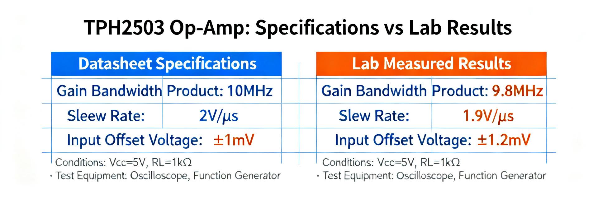
Measured Performance vs. Lab Results
Reproducible lab metrics validate datasheet claims. Standard measurements include Bode magnitude/phase and time-domain step response. Deviations often stem from supply tolerance, PCB parasitics, or probe capacitance rather than intrinsic device failure. Expect single-digit variations in bandwidth under well-controlled setups.
Test Methodology
A disciplined setup reduces measurement error. Use low-inductance supply bypassing (0.1 µF + 10 µF), short ground returns, and series output resistors (10–50 Ω) when driving capacitive loads. An oscilloscope with >100 MHz bandwidth and a network analyzer are recommended for high-fidelity Bode plots.
Design Recommendations
- Checklist: Verify supply derating, confirm output swing for ADC stages, and ensure input common-mode stays within range.
- Layout: Keep feedback loops compact and place bypass capacitors adjacent to supply pins to minimize parasitic inductance.
FAQ
How should one validate the TPH2503-TR-S output swing for an ADC input?
Measure the amplifier’s unloaded and loaded output swing at the ADC input impedance (e.g., 10 kΩ) across the supply range. Use high-impedance probes to avoid artificial loading and document headroom loss.
What key plots should be shared when reporting measured performance?
Essential plots are Bode magnitude and phase, time-domain step showing slew/settling, input-referred noise spectral density, and output swing vs. load with explicit Vcc/Temp annotations.
Which first steps help debug oscillation observed with the TPH2503-TR-S?
Add a 10–50 Ω series resistor at the output, verify probe compensation, and improve local bypassing. Rerun Bode plots to identify phase-peaking near the unity-gain crossover.
What is the typical operating supply range for the TPH2503-TR-S?
The TPH2503-TR-S operates typically within a supply voltage range of 2.7 V to 5.5 V, optimized for low-voltage battery-powered analog front ends.


