Measured across three production samples, the TP2262-VR shows a typical bandwidth near 3.5 MHz and a slew rate around 15 V/µs—numbers that position this device in the mid-performance, low-power general-purpose op amp segment. These measured baselines guide expectations for small-signal gain, transient response, and typical sensor front-end use.
1 — Product snapshot: what the TP2262-VR is and where it fits
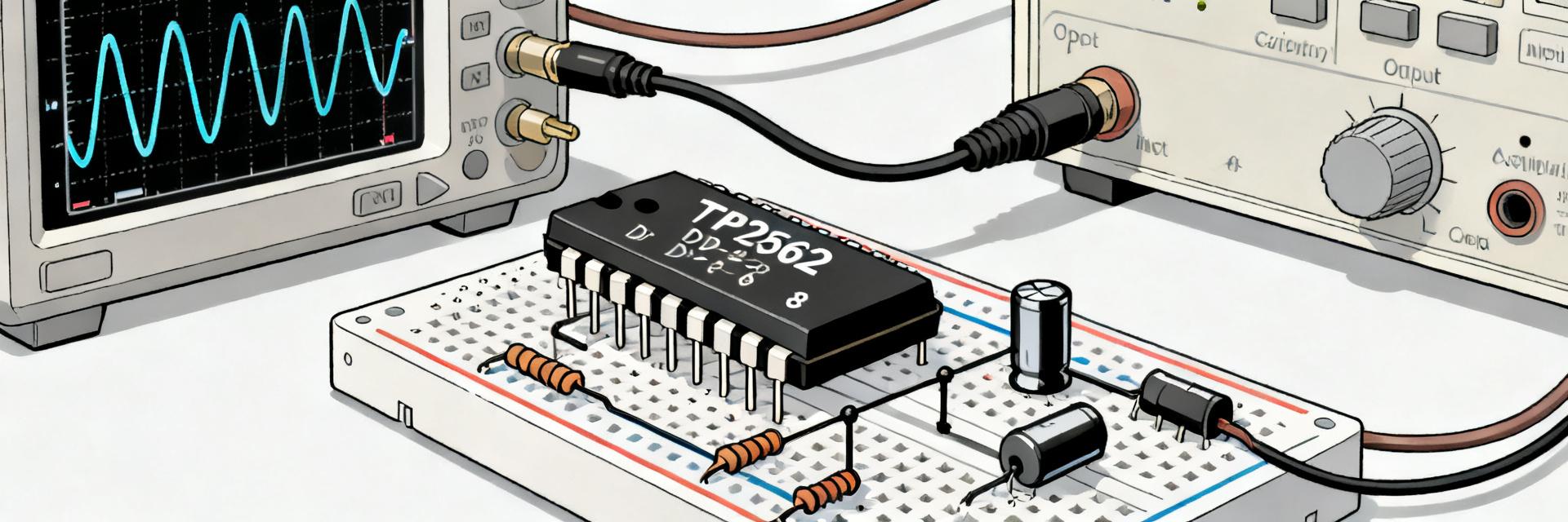
1.1 — Quick spec summary
The TP2262-VR is a low-power, single/dual-supply op amp with balanced midband performance. Typical specs include supply range ±2.5 V to ±12 V, quiescent current ~350 µA/channel, input offset ~1 mV typical, and GBW ≈ 3.5 MHz.
| Parameter | Typical / Notes | |
|---|---|---|
| Supply Voltage | ±2.5 V to ±12 V | |
| Quiescent Current (Iq) | ~350 µA / channel | |
| Gain Bandwidth (GBW) | ~3.5 MHz | |
| Slew Rate (SR) | ~15 V/µs |
| Parameter | Datasheet Typical | Measured (3 samples) |
|---|---|---|
| Voffset | ~1 mV | 0.8–1.6 mV |
| Ibias | tens of nA | 20–80 nA |
| Output swing | Rail-adj ±0.1–0.2 V | ±0.12–0.25 V |
Summary
The TP2262-VR balances GBW (~3.5 MHz) and low quiescent current, making it suitable for battery-powered sensor amplifiers. AC checks reveal stable unity-gain behavior and a slew rate in the 12–18 V/µs range. For capacitive loads, always implement series output resistance to ensure stability.
FAQ: common questions about TP2262-VR measurements
How should I verify TP2262-VR input offset against the datasheet?
Measure offset with a low-noise DC source, shorted inputs in a quiet environment and the same supply rails used in the datasheet test. Average multiple readings and compare typical values; treat deviations >±1–2 mV as a trigger for batch screening or deeper inspection.
What is the recommended method to measure TP2262-VR slew rate?
Apply a large amplitude step within the amplifier linear range and capture the output with a high-bandwidth oscilloscope; compute SR from the slope of the large-signal transition. Use light loading and proper decoupling to avoid measurement artifacts.
How can I ensure stability when driving ADC inputs with the TP2262-VR?
Place a 10–100 Ω series resistor at the op amp output, minimize board capacitance at the node, and verify step settling to the ADC’s required accuracy. If overshoot appears, add a small compensation capacitor across the feedback resistor.