
Introduction: The TPA2296T-S5TR appears in the datasheet with tight performance claims—wide supply range, sub-millivolt input offset and high common-mode rejection—but real boards often reveal gaps between sheet values and field behavior. This article walks through the most relevant datasheet specifications for the TPA2296T-S5TR, shows how to measure them, and explains practical limits to budget for in design verification.
1 — TPA2296T-S5TR at a glance: core datasheet claims (background)
1.1 Electrical operating ranges
Point: The datasheet enumerates nominal electrical operating ranges and those ranges drive system selection. Evidence: typical documents list a usable supply window, the allowed common‑mode voltage span and an industry-standard temperature grade. Explanation: confirm the exact supply voltage span, common‑mode upper limit and operating temperature range from the datasheet before committing to a topology—these determine allowed sense resistor choices and thermal management.
1.2 Highlighted performance numbers
Point: Headline specs are offset, CMRR, −3 dB bandwidth and slew rate. Evidence: each spec in the datasheet is accompanied by test conditions (supply voltage, ambient temperature, load or RL). Explanation: when comparing parts, always note test conditions — offset quoted at a single temperature and CMRR measured at a specified frequency can be optimistic relative to field conditions with varying common‑mode and temperature.
2 — Measured vs. datasheet: supply, offset and common‑mode behavior (data analysis)
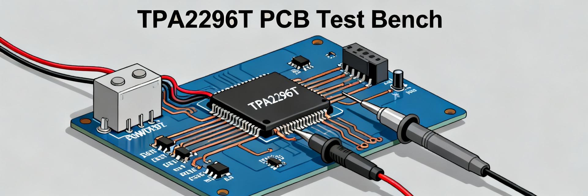
2.1 Lab setup and repeatable measurement method
Point: A reproducible setup is essential to separate device behavior from measurement artifacts. Evidence: use a small fixture with Kelvin sense, low‑noise power supplies, an isolated thermal sensor on the package and a calibrated low‑value sense resistor. Explanation: suggested steps—mount device on short‑trace PCB, use differential scope probes with common‑mode rejection, log ambient/junction temps, and define pass/fail relative to datasheet conditions.
2.2 Typical measurement deviations and tolerance analysis
Point: Expect measurable deviations from nominal values. Evidence: common observations include initial offset spread across parts, temperature drift and CMRR reduction at high common‑mode voltages. Explanation: present results with tables or plots: per‑lot mean and sigma, drift vs temperature, and common‑mode sweep; interpret discrepancies as either lot variation, biasing errors or measurement limitations.
3 — Noise, bandwidth and dynamic limits: practical measurements (data analysis)
3.1 Noise measurement: procedure and pitfalls — Point: Accurate noise measurement requires controlling the test bandwidth and noise floor. Evidence: specify measurement bandwidth (e.g., 0.1 Hz–100 kHz), use low‑noise supplies, and confirm the instrument noise floor by shorting inputs. Explanation: report RMS and PSD values referenced to the datasheet specifications, describe filtering and averaging used, and call out coupling or ground loop errors that commonly inflate measured noise.
3.2 Bandwidth, slew‑rate and transient response tests — Point: Dynamic performance affects stability with real loads. Evidence: measure −3 dB bandwidth with a sine sweep, and slew rate with a step stimulus at defined amplitude and load. Explanation: show both small‑signal BW and large‑signal slew; note effects of capacitive loads, input filtering and output stage limitations on rise/fall times and potential ringing or instability.
4 — How to test TPA2296T-S5TR on your bench: fixtures, calibration & thermal checks
4.1 Recommended fixtures, PCB considerations and probe techniques — Point: PCB and probe technique dominate measurement fidelity. Evidence: use short sense traces, Kelvin pads, solid ground islands and decoupling close to the supply pins. Explanation: recommended checklist—Kelvin sense resistor (10–100 mΩ), 0.1 µF and 10 µF decoupling, differential scope probes with tip‑to‑ground guarding, and scope bandwidth set 3–5× the expected device BW.
4.2 Calibration, thermal soak and common‑mode stress procedures — Point: Calibration and thermal control reveal true device behavior. Evidence: calibrate offset by measuring a known short, verify reference channels with a precision source, then thermal‑soak the board while monitoring package temperature with a thermocouple. Explanation: perform common‑mode stress sweeps slowly, allow thermal equilibrium between steps, and record offset and gain changes to capture drift mechanisms.
5 — Failure modes, limits seen in practice & troubleshooting examples
Point: Several predictable failure modes surface in testing. Evidence: symptoms include offset drift with temperature, output saturation near supply rails, reduced CMRR at high common‑mode, or oscillation with long input leads. Explanation: document observable indicators (dc shift, clipping, increased noise, sinusoidal artifacts) and initial checks such as measuring supply rails and probe grounding to rule out setup errors.
Point: A structured troubleshooting flow shortens debug time. Evidence: isolate the problem by swapping the device, replacing the PCB fixture and changing measurement gear. Explanation: corrective actions include improving decoupling, shortening sense traces, increasing sense resistance for better SNR, buffering the input or adding damping networks; suspect device lot issues only after eliminating fixture and measurement artifacts.
6 — Design checklist & margin rules when using TPA2296T-S5TR
- ✔ 6.1 Spec margin rules and derating guidance: Point: Derating key specs prevents field failures. Evidence: translate datasheet numbers into conservative production criteria—allow margin on supply headroom, extra offset allowance and temperature derating. Explanation: recommend safety margins in test criteria, e.g., define passing offset limits wider than nominal by the measured lot sigma and include temperature worst‑case in acceptance tests.
- ✔ 6.2 PCB layout, filtering and protection recommendations: Point: Layout and protection determine real‑world stability. Evidence: use ground islands, route sense traces away from noisy nets, add input series resistors and transient clamps as needed. Explanation: balance bandwidth and stability by choosing input filtering that keeps the loop stable under expected capacitive loads while meeting transient response requirements.
Summary
- Verify the TPA2296T-S5TR datasheet specifications against controlled bench tests: measure offset and CMRR with the same supply, temperature and load conditions cited in the datasheet to avoid misinterpretation.
- Adopt repeatable measurement fixtures—Kelvin sensing, low‑noise supplies, thermal monitoring—and log lot variation to set realistic production pass/fail criteria and derating rules.
- Prioritize layout and input protection: short sense traces, decouple near the device, and use input damping to preserve bandwidth without instability; build margin into offset and common‑mode allowances.
Article logistics & SEO notes: Meta suggestion: "Measured insights for the TPA2296T-S5TR: compare datasheet specifications with bench results, test methods, failure modes and design margins." Target searches around "TPA2296T-S5TR", "datasheet" and "specifications" should be covered by the headings and long‑tail phrases used in the section intros and measurement guides above.


