
The TP2581-TR datasheet highlights a practical rail-to-rail, single-supply amplifier aimed at sensor front-ends and ADC drivers; key published figures include a typical bandwidth of 10 MHz and a slew rate of 8 V/µs (datasheet: 10 MHz typical bandwidth; datasheet: 8 V/µs slew rate). This article’s purpose is a concise, data-driven deep dive: how to extract the right datasheet fields, run repeatable benchmarks, and apply design tips and test methods engineers can use immediately.
1 — Quick Overview: What the TP2581-TR Is and Where it Fits
Specification snapshot (one-line TL;DR)
Point: Provide a single-scan spec table for decision-making. Evidence: extract these fields from the datasheet so readers can compare parts quickly. Explanation: include supply range, input type, rail-to-rail I/O, bandwidth, slew rate, supply current and package for rapid screening.
| Parameter | Value (from datasheet / note) |
|---|---|
| Supply voltage range | datasheet: pull Vmin — Vmax (record min/max) |
| Input type | Single-supply, single-ended inputs (record common‑mode range) |
| Rail-to-rail I/O | Yes (verify input common‑mode vs rails and output swing) |
| Bandwidth | datasheet: 10 MHz typical bandwidth |
| Slew rate | datasheet: 8 V/µs |
| Supply current | datasheet: quiescent current per amplifier (record typ/max) |
| Package | SOT‑23‑5 |
Typical application domains and target uses
Point: Match strengths to domains. Evidence: rail‑to‑rail I/O and single-supply operation suit portable and industrial sensor front-ends. Explanation: list scenarios — (1) low-voltage industrial sensors needing <1 mV offset and rail access; (2) ADC drivers in portable test equipment requiring stable drive up to a few MHz; expected performance needs: low offset, moderate bandwidth, and careful layout to hit datasheet numbers.
2 — Electrical Characteristics & Pinout Explained
Key DC specs: offsets, bias, input/output ranges
Point: DC rows determine precision. Evidence: pull input offset, offset drift, input bias current, and common‑mode range from the datasheet. Explanation: for low-voltage single-supply systems, ensure the amplifier’s input common‑mode includes the sensor output; offset and drift drive calibration and trimming choices, and input bias affects high‑impedance sensor sources.
AC specs: bandwidth, slew rate, gain-bandwidth product
Point: AC specs set signal-chain limits. Evidence: datasheet: 10 MHz typical bandwidth and datasheet: 8 V/µs slew rate. Explanation: closed‑loop bandwidth ≈ GBW / closed‑loop gain; for example, at unity closed loop expect near the 10 MHz region, while at gain = 10 expect ~1 MHz. Slew rate limits large-step settling: for a 2 Vpp step, rise time ≈ (2 V) / (8 V/µs) = 0.25 µs, implying designers must check slew‑limited distortion in time‑domain tests.
3 — Performance Benchmarks: Real-World Behavior
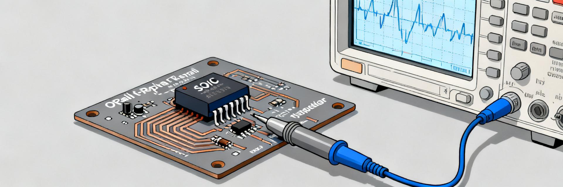
Bench test plan & setup
Point: A repeatable test plan removes ambiguity. Evidence: align test conditions with datasheet (supply rails, ambient temp, load). Explanation: recommended setup — low‑noise power supply, 0.1 µF + 10 µF decoupling near Vcc, 1 kΩ load for output swing checks, use 50 Ω source only when specified; measure bandwidth with a network/FFT analyzer, slew with a fast pulse generator and 1 MΩ load to avoid extra loading.
Interpreting benchmark results vs datasheet claims
Point: Differentiate typical vs guaranteed. Evidence: datasheet typically lists typ/min/max. Explanation: report measured typical alongside datasheet typical and limits; discuss margins if measured bandwidth falls 10–30% below datasheet—common causes include layout inductance, insufficient decoupling, or high source impedance; document probe loading and cable effects.
4 — Practical Design Considerations & Application Circuits
Sample circuits and PCB/layout tips
Point: Two compact reference circuits aid adoption. Evidence: typical use is inverting sensor conditioner and non‑inverting ADC buffer. Explanation: include these quick tips — keep input traces short, place decoupling within 2 mm of Vcc pin, route input guard traces for high‑impedance sensors, and isolate analog ground islands from digital return paths. Use 10–100 nF in parallel with 4.7 µF for decoupling.
Stability, compensation and load-driving guidance
Point: Practical loads affect stability. Evidence: capacitive loads and heavy cable capacitance can introduce phase lag. Explanation: add small series output resistor (10–100 Ω) to isolate capacitive loads, consider feedback compensation (small C across feedback resistor) if peaking appears, and respect output swing limits near rails shown in the datasheet when driving low‑impedance loads.
5 — Comparative Case Studies: TP2581-TR in Real Designs
Two short case studies (concise, practical)
Point: Real designs reveal tradeoffs. Evidence: Case A — sensor front‑end prioritized low offset and single‑supply headroom; Case B — ADC buffer emphasized bandwidth and low distortion. Explanation: for Case A, designers used gain of 10, trimmed offset in software and achieved sub‑mV accuracy after layout improvements; for Case B, careful short traces and local decoupling recovered bandwidth near datasheettypical values while keeping THD low.
When to pick the TP2581-TR (trade-offs)
Point: Define selection checkpoints. Evidence: strengths are wide single‑supply compatibility, rail‑to‑rail I/O, and modest 10 MHz-class bandwidth. Explanation: choose this part when you need rail access and moderate bandwidth; avoid it for very high‑frequency or RF front ends where GBW and noise floor are insufficient.
6 — Benchmarks Checklist & Test Methodology
Step-by-step bench checklist
- Verify rails and decoupling (0.1µF + 10µF).
- Confirm open-loop offset before dynamic testing.
- Measure unity gain response & step to gain settings.
- Run slew and settling tests with 10x probe.
- Document load and probe compensation clearly.
Explanation: measurement sequence — verify rails and decoupling, confirm open‑loop offset, measure unity gain response, step to gain settings, run slew and settling tests, document load and probe compensation; annotate test points and use 10× probe with short ground spring to reduce error.
Suggested test report & datasheet comparison template
Point: Standardized reporting improves communication. Evidence: a simple table of spec vs. measured helps readers compare. Explanation: include columns — parameter, datasheet value (typ/min/max), measured typical, measurement conditions, notes on deviation and corrective actions; add suggested long‑tail SEO sentences when publishing measured benchmarks.
Common Questions
What supply range does TP2581-TR support and how does that affect precision?
Datasheet supply limits determine allowable headroom; operate within specified Vmin–Vmax and verify input common‑mode includes sensor outputs. Precision is affected by offset and drift—compare datasheet offset/drift rows and measure at expected ambient and supply conditions to confirm performance.
How should benchmarks be reported vs the datasheet for publication?
Report measured typical values alongside datasheet typical and limits, include test conditions (supply, load, probe type, temperature), and note layout or probe effects. Use a table comparing parameter, datasheet value, measured value and deviation with corrective notes.
What layout and probing tips reduce measurement error when testing TP2581-TR?
Place decoupling within millimeters of supply pin, use short ground springs on oscilloscope probes, minimize input loop area, and avoid long cables on outputs. These steps reduce parasitics that otherwise lower measured bandwidth and increase settling time compared to datasheet benchmarks.


