
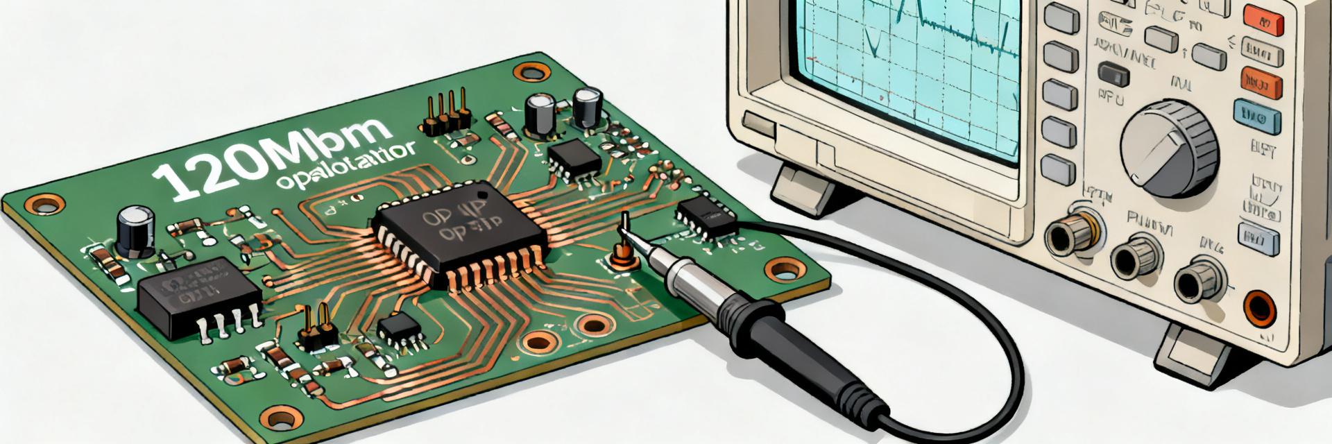
Point: The TPH2501-TR delivers a compelling balance of speed and low-voltage compatibility for embedded designs.
Evidence: The datasheet specifies ~120 MHz GBW, ~200 V/µs slew rate, rail-to-rail I/O, and guaranteed operation from 2.5–5.5 V.
Explanation: Those numbers signal a wideband, low-voltage amplifier suitable for buffering and front-end stages where both bandwidth and single-supply operation matter; this article explains what the specs mean in practice, how to measure them, and when to choose the part. (TPH2501-TR, op amp, performance)
Point: Readers will get hands-on guidance rather than abstract claims.
Evidence: Each section translates datasheet figures into expected closed-loop bandwidth, settling behavior, and test setups.
Explanation: The structure follows product background, datasheet deep-dive, measurement best practices, integration tips, and actionable checklists so engineers can validate performance on the bench.
1 — Product background and where it fits
Quick specs snapshot to lead the section
Point: A concise spec snapshot sharpens positioning. Evidence: key typical figures from the vendor datasheet are summarized below. Explanation: use this table to pick the right class of amplifier for your system-level needs.
| Parameter | Typical / Range (datasheet) |
|---|---|
| Supply range | 2.5 – 5.5 V |
| Gain-Bandwidth (GBW) | ~120 MHz |
| Slew rate | ~200 V/µs |
| Rail-to-rail I/O | Yes (typical) |
| Quiescent current | Low, datasheet typical |
| Input bias / offset | Low bias, offset specified (datasheet) |
| Output drive | Moderate drive for small loads |
| Package | Small SMD packages (see datasheet) |
Point: The TPH2501-TR aligns with wideband, low-voltage, RR I/O amplifier classes. Evidence: GBW and slew figures place it above general-purpose op amps and below specialty RF parts. Explanation: US engineers will consider it for signal-chain blocks that need multi-MHz closed-loop bandwidth on 3.3 V rails while retaining rail-to-rail swing for single-supply systems.
Typical target applications and why
Point: Match spec to application. Evidence & explanation: example fits include:
- Portable instrumentation — GBW and RR I/O enable high-speed readings on 3.3 V battery systems.
- Sensor front-ends — low supply and rail-to-rail capability simplify single-supply sensor interfaces (suggested phrase: "TPH2501-TR op amp for sensor front end").
- High-speed buffering for ADC drivers — wideband and fast slew reduce pre-ADC distortion at sampling edges.
- Signal conditioning in handheld test equipment — balanced speed and power for longer runtime.
2 — Datasheet deep-dive: key electrical metrics and interpretation
Frequency- and time-domain specs: what matter and why
Point: GBW, -3 dB bandwidth, and slew rate each constrain different performance axes. Evidence: GBW (~120 MHz) yields closed-loop bandwidth = GBW / closed-loop gain; slew rate (~200 V/µs) limits large-signal edge speed. Explanation: for example, expected closed-loop -3 dB bandwidth is ~120 MHz at gain=1, ~12 MHz at gain=10, and ~1.2 MHz at gain=100. For a 2 V step, slew-limited rise ≈ 2 V / 200 V/µs = 10 ns, affecting settling for fast ADC drives.
Input/output, noise, and offset details that affect system-level accuracy
Point: Input bias, offset, and output swing map directly to DC and low-frequency errors. Evidence: datasheet specifies input offset and bias (typical/max) and output swing margins near rails. Explanation: translate specs into error: if input bias = 1 nA and source impedance = 10 kΩ, bias-induced error ≈ 10 µV. If input offset = 200 µV and closed-loop gain = 10, output DC error ≈ 2 mV; include offset drift when your application sees temperature changes.
3 — Benchmarking & measurement best practices
Recommended test setups and measurement parameters
Point: Accurate bench verification requires controlled setups. Evidence: common practice uses single-point supplies (3.3 V typical), 50 Ω load or defined resistive loads, and high-bandwidth scopes. Explanation: use a 50 Ω or 1 MΩ oscilloscope input as appropriate, prefer active probes with >200 MHz bandwidth or 10× passive probes with probe compensation, place decoupling at the package, and use sine sweeps for small-signal GBW and fast step generator for slew/settling.
Interpreting typical datasheet graphs vs. bench results
Point: Bench results often deviate from datasheet curves due to parasitics. Evidence: scope probe capacitance, fixture inductance, and supply decoupling change measured gain and phase. Explanation: checklist for reproducing curves: minimize trace inductance, use proper decoupling (0.1 µF + 1 µF close to pins), use short ground leads on probes, and accept typical-tolerance bands (±10–20% for typical curves versus guaranteed limits for max/min specs).
4 — Design & integration guide
PCB layout, decoupling, and power considerations for best performance
Point: Layout makes or breaks wideband op amp performance. Evidence: datasheet performance assumes low parasitics and good decoupling. Explanation: keep input/fb traces shortest, use a continuous ground plane, place 0.1 µF ceramic decouplers within 1–2 mm of supply pins complemented by 1 µF bulk capacitors, and provide thermal vias under exposed pads if present to manage power dissipation under load.
Circuit-level tips: configuring gains, compensation, and driving loads
Point: Stability and noise depend on feedback components and source/load impedances. Evidence: high closed-loop gains reduce bandwidth and can improve noise; large feedback resistances increase noise and offset sensitivity. Explanation: prefer feedback resistors in the 1 kΩ–100 kΩ range depending on noise and bias trade-offs; for unity-gain buffer, expect full GBW and best phase margin; for noninverting gain-of-10, choose R1=1 kΩ, Rf=9 kΩ (example) for a balance of noise and loading. Recommended output loads: avoid heavy capacitive loads without isolation resistor (e.g., 50–100 Ω series) to prevent ringing.
5 — Application case studies and practical action checklist
Two short use-case sketches
Point: Concrete sketches clarify suitability. Evidence & explanation:
Example A — Precision sensor amplifier
Requirements: low offset, rail-to-rail I/O, low supply 3.3 V. Why it fits: RR I/O and low-voltage operation simplify reference and ADC interfacing. Pointer: single-supply noninverting stage with input filtering.
Example B — High-speed driver for ADC input
Requirements: few-MHz bandwidth, low settling to 0.1% in a few 100 ns. Why it fits: GBW supports multi-MHz closed-loop gains and slew supports fast edges. Targets: closed-loop bandwidth, 0.1% settling time.
10-point implementation checklist
- Verify supply-voltage headroom per datasheet.
- Place decoupling (0.1 µF + 1 µF) adjacent to supply pins.
- Confirm closed-loop bandwidth with a swept sine test.
- Measure slew-induced distortion with large-step test.
- Validate input bias under expected source impedance.
- Test output swing under worst-case load.
- Run thermal check at maximum expected dissipation.
- Confirm ADC/comparator interface timing and settling.
- Perform board-level EMI checks around high-speed nodes.
- Document pass/fail criteria and record measured vs. datasheet values.
Summary
Point: The TPH2501-TR is a practical choice when you need a wideband, low-voltage op amp with rail-to-rail I/O that simplifies single-supply designs while delivering multi-MHz closed-loop bandwidth. Evidence: datasheet GBW (~120 MHz), slew (~200 V/µs), and 2.5–5.5 V operation. Explanation: validate the part on the bench using the measurement setups and checklist above before production to ensure the expected bandwidth, settling, and DC accuracy meet system requirements. For engineers: consult the official datasheet and run the provided checklist before committing to a design. (TPH2501-TR)
- TPH2501-TR offers ~120 MHz GBW and ~200 V/µs slew, enabling unity-gain bandwidth and multi-MHz closed-loop designs.
- Measure GBW with low-parasitic fixtures and calculate closed-loop bandwidth as GBW / gain.
- Translate input bias and offset into voltage error using source impedance.
- Use tight PCB layout, close decoupling, and series output isolation for capacitive loads.
Guidance for writers
How to interpret TPH2501-TR performance targets during a design review?
Point: Focus review on measurable system-level specs. Evidence: datasheet typical vs. max values can differ; measurement setup affects results. Explanation: require that reviewers confirm test conditions (supply, load, probe, temp) match datasheet test conditions, verify closed-loop bandwidth at the target gain, check slew-induced settling for worst-case steps, and record deviations with potential mitigations before sign-off.
What bench artifacts most commonly produce discrepancies from datasheet performance?
Point: Parasitics and measurement technique cause most visible differences. Evidence: probe capacitance, ground loops, and inadequate decoupling show up as roll-off, overshoot, or noise. Explanation: mitigate by using short ground connections on probes, active probes when needed, proper decoupling, and repeating measurements with different loads to isolate fixture effects.
Which final tests should be automated before production sign-off?
Point: Automate repeatable, pass/fail criteria. Evidence: automated test saves time and enforces consistency. Explanation: include automated checks for DC offset under expected source conditions, closed-loop bandwidth sweep, large-step slew/settling time, output swing under load, and thermal drift tests; log results and compare to acceptance thresholds from the checklist above.


