
The TPA1286 datasheet highlights three practical, design-impacting takeaways: a broad accepted supply range that eases integration with common sensor rails, a single‑resistor gain architecture that simplifies gain programming, and low offset/zero‑drift performance that minimizes calibration work in production. Each of these metrics directly reduces board‑level complexity — supply flexibility shortens power-rail design cycles, resistor‑set gain lowers BOM and layout risk, and low offset improves end‑product accuracy without repeated trimming. This deep‑dive covers the spec highlights, pinout clarity, design tips, and a test checklist so engineers can integrate the part with fewer surprises and faster time to first pass. For the official numbers and application diagrams, download the manufacturer’s datasheet from the vendor or authorized distributor pages (search for the TPA1286 datasheet on the supplier site).
1 — Background: What the TPA1286 is and where it fits
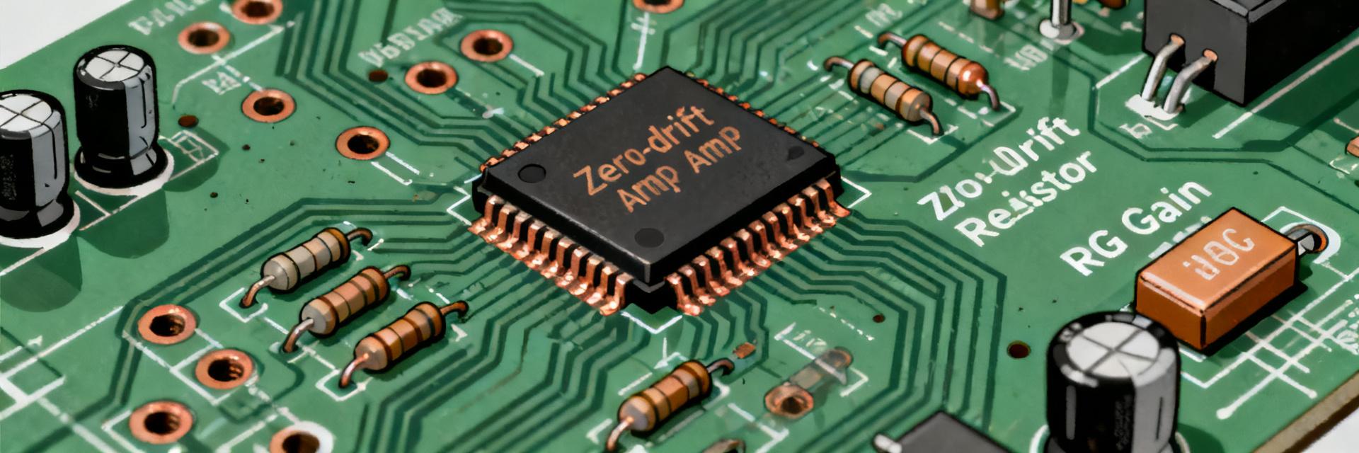
The TPA1286 is presented in the datasheet as a precision instrumentation amplifier with zero‑drift architecture, intended for high‑accuracy sensor front ends. Its zero‑drift core targets ultra‑low offset and long‑term stability, which makes it a fit for data‑acquisition, industrial instrumentation, and medical sensing where microvolt‑level errors matter. Designers select this device when they need a small, single‑component instrumentation solution that replaces multi‑op‑amp front‑ends while preserving precision and reducing component count.
1.1 Core function and typical applications
As an instrumentation amplifier / zero‑drift amplifier, the TPA1286 provides differential measurement with high input common‑mode rejection. Typical applications include strain gauge and bridge sensor interfaces (where low offset and drift limit system recalibration), 4–20 mA loop receivers when paired with appropriate front‑end conditioning, and portable data loggers that benefit from single‑resistor gain control. The datasheet calls out bridge excitation compatibility and low‑noise input stages as supporting claims for these use cases.
1.2 Key differentiators (from the datasheet)
The datasheet emphasizes a compact single‑resistor gain setting, a wide supply span for flexible systems, low input offset and drift from the zero‑drift topology, and solid output drive capability. Compared with generic op amp solutions, these attributes reduce external parts and board area while maintaining accuracy: single‑resistor gain removes matched resistor networks, wide supply span permits single‑supply operation near common sensor rails, and low drift reduces long‑term calibration. See the TPA1286 datasheet for manufacturer‑stated comparative curves and application notes.
2 — Top-line specs: TPA1286 specs at a glance
The essential electricals to extract from the datasheet are: supply voltage range, input offset and drift, input bias current, gain range and setting method, input common‑mode range, output swing and output current, and bandwidth/slew rate. Below is a compact spec table mapping each parameter.
| Parameter | Symbol | Typical / Limit | Units |
|---|---|---|---|
| Supply voltage range | VCC | See datasheet | V |
| Input offset (typ / max) | VOS | See datasheet | µV |
| Offset drift | dVOS/dT | See datasheet | µV/°C |
| Input bias | IB | See datasheet | pA / nA |
| Gain setting | RG → G | Single‑resistor formula | — |
| Common‑mode range | VCM | See datasheet | V |
| Output swing / drive | VOUT, IO | See datasheet | V, mA |
| Bandwidth / Slew rate | BW / SR | See datasheet | Hz / V/µs |
2.1 Electrical characteristics to extract and present
When documenting TPA1286 specs for selection, explicitly extract the exact supply limits, offset and drift numbers, input bias current, gain conversion formula, common‑mode range, output swing and current, and bandwidth figures. Label each entry with symbol, typical value, and guaranteed limit. Use the secondary keyword "TPA1286 specs" in the specification caption when publishing tables or BOM notes to help engineers find the right reference quickly.
2.2 Performance metrics and real-world implications
CMRR and PSRR tell how much common‑mode and supply noise will appear at the output — prioritize high CMRR for bridge sensors and high PSRR for battery‑powered or noisy power rails. Noise density and bandwidth determine measurable resolution: low noise favors high‑resolution ADCs, while higher bandwidth favors dynamic sensors. For low‑noise designs prioritize offset, drift, and noise; for fast systems prioritize slew rate and bandwidth. Add a "specs to verify in production testing" callout for these metrics.
3 — Pinout and package: reading the TPA1286 pinout correctly
Correct pin handling prevents common integration failures. The datasheet pinout and recommended land pattern identify sensitive nodes such as REF, gain resistor node, power pins, inputs and outputs. Follow recommended decoupling and keep sensitive input traces short and shielded from digital switching. The term "TPA1286 pinout" should be used in captions of any layout or assembly notes to surface the pinmap in documentation.
3.1 Pin-by-pin functions and recommended PCB footprint notes
Provide a pin table mapping: pin number, name, function, and recommended connection. Call out: VCC → local decoupling to ground; GAIN/REF node → short trace to external resistor and to reference bypass; inputs → guarded traces and low‑leakage routing; outputs → route to ADC with series resistor if needed. Include a clearly labeled footprint in your library matching the manufacturer land pattern and tolerance guidance.
3.2 Thermal, package variants and mechanical considerations
Summarize available packages and any thermal limits noted in the datasheet; consult junction‑to‑ambient thermal resistance values when planning copper pours or thermal vias. Best practices: add thermal vias under exposed pads, use solid ground pours with stitching, and keep analog return paths short. Verify mechanical tolerances against your pick‑and‑place and stencil processes before final BOM freeze.
4 — Design & implementation guidance
Practical guidance accelerates stable first prototypes: calculate gain with the datasheet formula, select low‑TC resistors, follow recommended decoupling, and apply input protection based on expected sensor transients. Below are focused tips for gain setting and power/layout best practices.
4.1 Gain setting, resistor selection and input conditioning
Use the exact gain resistor formula provided in the datasheet to compute RG from desired gain; choose precision resistors (≤0.1% tolerance, low ppm/°C) to preserve gain accuracy. Consider adding small input RC filters to limit input bandwidth and protect against aliasing; add series protection (resistors, TVS) for harsh environments. Document resistor selection in your error budget to quantify offset and gain error impact on system accuracy.
4.2 Powering, decoupling, and layout best practices
Follow the datasheet decoupling recommendations: place a low‑ESR 0.1 µF ceramic immediately between VCC and GND at the device pins, plus a bulk capacitor nearby. Observe power sequencing notes if present, and add transient protection for supply transients. PCB checklist before prototyping: verify decoupling placement, confirm gain resistor footprint, and ensure analog and digital returns are separated until a single convergent ground plane.
5 — Testing, validation & troubleshooting checklist
A structured validation plan shortens the debug loop. Bench tests should measure offset, drift, CMRR, PSRR, gain accuracy, and bandwidth under controlled conditions, and compare results to the datasheet’s typical and guaranteed values. Include pass/fail thresholds and repeatability checks to catch layout‑induced issues early.
5.1 Bench test setup and measurement checklist
Recommended bench setup: low‑noise DC supply, precision source for differential inputs, high‑resolution ADC or nanovolt meter, and temperature control if drift testing. Top six measurements: offset, offset drift, CMRR, PSRR, gain accuracy at multiple gains, and bandwidth. Use guarded cabling and minimize test jig leakage to reduce measurement error; document expected pass/fail thresholds derived from the datasheet.
5.2 Interpreting datasheet limits vs. real-world performance and debug tips
If your board fails to meet datasheet numbers, common causes include inadequate decoupling, long/unshielded input traces, incorrect gain resistor value, or test setup errors. Debug by swapping bypass caps, shortening input traces, isolating the input source, and verifying resistor values and solder joints. Capture before/after measurements to confirm root‑cause.
FAQ
What key specs in the TPA1286 datasheet should I verify first?
Start with supply voltage range, input offset and drift, gain setting method, and output swing/drive. These determine whether the device will interface correctly with your sensors and ADC and whether it meets your accuracy budget. Verify these on the bench under the same conditions listed in the datasheet.
How do I calculate the external gain resistor for the TPA1286?
Use the gain formula provided in the datasheet (RG → G relationship). After computing RG for your target gain, pick a precision resistor with low temperature coefficient and verify the actual gain on the bench. Document resistor tolerance impact in your system error budget.
Where can I find the recommended PCB footprint and pinout for the TPA1286?
The manufacturer’s datasheet includes the recommended land pattern, pinout diagram, and notes on special pins (REF, gain node). Use that land pattern in your CAD library and follow the decoupling and keep‑out measurements indicated to prevent layout‑related performance issues.


