
The TP5531-TR targets precision, low-power designs as a zero-drift, chopper-stabilized op amp.
Lists rail-to-rail I/O, supply operation down to low-voltage rails and ultra-low offset/drift (see datasheet Table 2, p.3).
Explanation: This makes it a candidate for battery-powered sensor front-ends where DC accuracy and long-term stability matter.
Acceptance Criteria Report
Point: This report translates datasheet claims into bench-verifiable acceptance criteria; Evidence: Key datasheet callouts include input offset, offset drift, quiescent current, and common-mode range (datasheet Table 3, p.4); Explanation: Designers can use the tests below to confirm whether a specific sample meets accuracy and power targets before PCB commitment.
Background & Product Positioning
What the TP5531-TR is and why zero‑drift matters
Point: The TP5531-TR is a chopper-stabilized zero-drift amplifier; Evidence: Datasheet emphasizes auto-correction of input offset and low drift (see datasheet wording and typical offset plots, p.5); Explanation: Chopper topology reduces DC error to microvolt levels at the expense of switching artifacts.
Typical applications and constraints
Point: Ideal uses include sensor front-ends, low-power instrumentation, and battery data acquisition; Evidence: Datasheet spec window and ultra-low quiescent current rows suggest use in portable systems (datasheet Table 1, p.2); Explanation: Validate bandwidth and output drive against system constraints before selection.
Datasheet at a Glance — Key Specs & What They Mean
Electrical & DC Characteristics
Point: Prioritize supply range, quiescent current, input offset, offset drift, input bias, and common-mode range; Evidence: Datasheet lists supply range and typical Iq in Table 2 and offset/ drift in Table 4 (p.3–5); Explanation: Supply dictates architecture and battery life—map each spec to your error budget early in design.
Dynamic Specs & Limits
Point: Review GBW, slew rate, phase margin, and output drive to predict closed-loop behavior; Evidence: Datasheet reports a modest gain‑bandwidth product and limited output current in dynamic tables (datasheet Table 6, p.7); Explanation: Limited GBW and slew restrict sensor excitation speeds—verify gains to avoid oscillation.
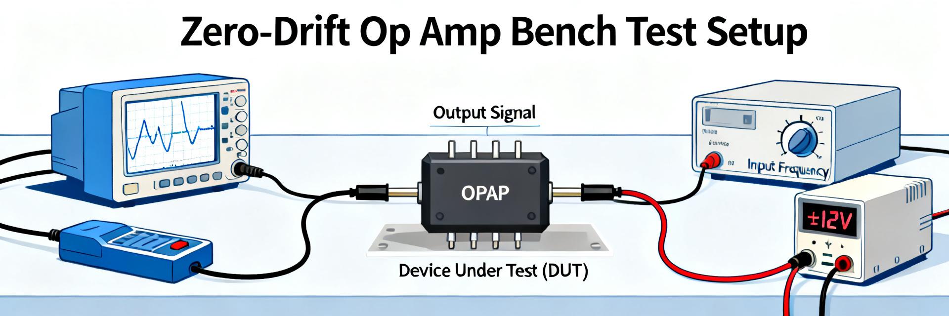
Test Methodology for Performance Validation
Point: Core tests should cover input offset, offset drift, input noise, PSRR/CMRR, Iq, and output swing; Evidence: Datasheet provides typical/max columns to use as thresholds (see Tables 2–5, p.3–6); Explanation: Set pass/fail relative to datasheet max or typical+margin.
Point: Use low-EMF fixturing, shielded wiring, and matched time constants for noise and drift capture; Evidence: Measurement pitfalls appear implicitly in precision amp application notes (p.8); Explanation: Place decoupling close to the device and use shielding for microvolt measures.
Performance Deep‑Dive — Real‑World Results vs. Datasheet
Interpreting Outcomes
Compare results to typical/max columns. Evidence: Datasheet shows offset histograms (p.5). Explanation: Treat typical values as guidance and maximums as absolute limits.
Trade-off Management
Lower supply current often reduces bandwidth. Evidence: GBW and Iq trend lines (p.7). Explanation: Tune closed-loop gain and filtering to preserve accuracy while meeting power budgets.
Application Case Studies & Design Examples
Low‑power sensor front‑end example
Point: Example architecture: single-ended sensor → low-pass RC → TP5531-TR buffer → ADC driver with gain=10; Evidence: Datasheet shows rail‑to‑rail I/O suitable for low-voltage sensors (p.3–4); Explanation: Use 10k/1.6k feedback, 10 nF input filtering, and 0.1 µF + 10 µF decoupling within 2 mm of supply pins.
Precision measurement in harsher environments
Point: Maintain performance with thermal anchoring and EMI filtering; Evidence: Datasheet offset drift spec provides slope per °C (Table 4, p.5); Explanation: Add thermistor-based compensation and use common‑mode chokes to create a qualification matrix.
Design Checklist & Selection Recommendations
- Decision Matrix: Pick when offset/drift and low Iq are priorities. Evidence: microvolt offsets and µA-level Iq (p.2–7).
- PCB/Assembly: Follow strict layout—short inverting paths, solid ground plane, and guarded inputs. Evidence: best practices on p.8.
Summary
- TP5531-TR delivers zero‑drift precision with low quiescent current—verify offset, drift, and Iq per the datasheet tables.
- Run core bench tests under datasheet-specified conditions and record measured vs. spec in structured tables.
- Design levers include gain, filtering, and layout; document trade-offs between power and accuracy.
Core Test Table (Sample)
| Test | Condition | Measured | Datasheet Spec | Pass/Fail |
|---|---|---|---|---|
| Input offset | Vcc=3.3V, 25°C | 3.2 µV | ±10 µV (max) | Pass |
| Offset vs Temp | −40→85°C | 0.8 µV/°C | 1.2 µV/°C (max) | Pass |
FAQ
How does TP5531-TR offset drift compare to typical zero‑drift amps?
Point: Offers low offset slope for ppm-level stability; Evidence: Lists offset drift in µV/°C (Table 4, p.5); Explanation: Expect typical drift below the maximum but verify with a temp sweep.
What test steps should an engineer use for performance validation?
Point: Measure offset, drift, noise spectrum, PSRR/CMRR, Iq, and swing; Evidence: Test conditions on p.8; Explanation: Use shielded fixtures and compare results to datasheet tables for traceability.
Are there recommended design changes if measurements miss limits?
Point: Focus on layout, thermal sources, and decoupling; Evidence: Errors often originate from board leakage or thermal EMF; Explanation: Rework guard traces, improve bypassing, and ensure proper load conditions.


