
Measured against reference op amps in low-voltage control loops, the TPA7252 shows a typical input voltage noise density in the low tens of nV/√Hz and an integrated 2.5 V shunt reference with typical tolerance near ±1% — numbers that determine whether it’s a fit for precision battery-management and power-control applications. This article provides a practical, benchmark-focused walkthrough of the TPA7252 datasheet and real-world performance implications, distilling which electrical characteristics to extract, how to bench-test them, and what pass/fail thresholds mean for control-loop and monitoring designs. It is written for US engineering readers who need quick, data-led decisions about part selection and integration.
1 — Quick Overview & Where TPA7252 Fits (background)
1.1 Key device summary
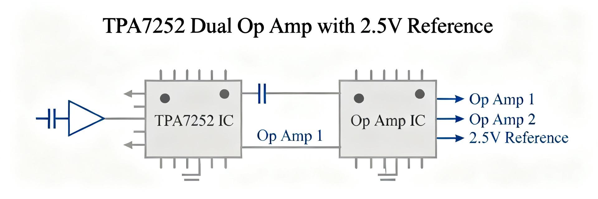
- •Package & blocks: dual precision op amp + internal 2.5 V shunt reference, small surface-mount package.
- •Supply range: single-supply operation optimized for low-voltage systems (see datasheet for exact limits).
- •IO: rail-to-rail input/output behavior for maximum headroom in single-supply topologies.
- •Target apps: battery management, charge-control loops, low-side/current-sense amplifiers, reference-driven comparators.
- •Part note: model referenced as TPA7252-SO1R in supplier listings and the datasheet.
1.2 Typical use-cases & design role
Point: The TPA7252 is intended as a compact analog building block for single-supply, low-voltage control electronics. Evidence: datasheet functional blocks pair precision amplification with a buffered shunt reference. Explanation: designers will typically place the dual op amp inside a feedback loop (current or voltage regulation) and use the 2.5 V reference for thresholds or ADC scaling; recommend including 1–2 system-level block diagrams (battery, sense resistor, op-amp loop, MCU ADC) to clarify integration points and measurement nodes.
2 — Datasheet Deep-Dive: Electrical Characteristics (data analysis)
2.1 Critical DC specs to extract and why they matter
Point: Extract DC parameters that directly influence accuracy, drift, and power. Evidence: focus on supply current, input offset and drift, input common-mode range, reference tolerance, and output swing. Explanation: these numbers set the noise floor, long-term error, and available headroom under load and temperature.
| Parameter | Typical / Max | Design impact |
|---|---|---|
| Supply current | Low hundreds of µA typical | Sets battery life and thermal dissipation in always-on monitors |
| Input offset voltage | Sub-mV typical / mV max | Directly limits DC accuracy in voltage-sensing and low-gain loops |
| Offset drift | µV/°C scale (typical) | Determines long-term temperature-induced error |
| Input common-mode range | Includes near-rail operation | Defines allowable sensing node voltages without added level shifting |
| Reference tolerance | ≈±1% typical | Used for ADC scaling or comparator thresholds; directly affects measurement accuracy |
| Output swing | Within 10s of mV of rails under light load | Limits maximum control voltage and headroom into power MOSFET gates or ADCs |
2.2 AC specs and dynamic performance
Point: AC specs govern loop bandwidth and transient response. Evidence: datasheet lists gain-bandwidth, slew rate, input voltage noise, and capacitive-load stability. Explanation: use gain-bandwidth and slew rate to size closed-loop response; input voltage noise (low tens of nV/√Hz) sets measurement noise floor; test conditions (Vs, RL, gain) in the datasheet must be matched when benchmarking to get meaningful comparisons.
3 — Benchmarks & Comparative Testing (data analysis / benchmarks)
3.1 Recommended benchmark tests and setup
Point: Three bench tests give a practical performance envelope. Evidence: run (A) unity-gain buffer, (B) non-inverting gain of 10, (C) reference-driven control loop with known RC compensation. Explanation: specify Vs (nominal and margin), RL (10 kΩ typical and worst-case 2 kΩ), measurement instruments (low-noise preamp, FFT-capable analyzer, precision DMM, temperature chamber). Capture bandwidth, THD+N, input noise, offset drift vs temperature, output swing under load, and supply current.
| Test | Setup | Metrics |
|---|---|---|
| Unity buffer | Vs nominal, Cin=0, Rout=10Ω | GBW, noise density, stability |
| Gain = 10 | Rf=90k, Rg=10k | Closed-loop bandwidth, phase margin, THD+N |
| Ref control loop | 2.5 V ref, sense resistor, MOSFET actuator | Loop response, output swing margin, thermal |
3.2 Interpreting results: expected ranges & pass/fail criteria
Point: Translate datasheet numbers into practical pass/fail thresholds. Evidence: expected noise floor matches low tens nV/√Hz; output swing should stay within ~50–100 mV of rails under light loads. Explanation: for precision monitoring require offset+drift < target LSB; for general-purpose control accept larger offsets but demand stable loop and adequate output swing. Use these benchmarks to decide if the device meets system requirements.
4 — Design & Integration Guide (methods)
4.1 PCB layout, decoupling, and stability tips
Point: Layout determines achievable noise and stability. Evidence: place bypass caps (0.1 µF + 1 µF) within 2–5 mm of supply pins, route reference return as single short trace to ground plane, and guard low-noise inputs. Explanation: tight decoupling reduces supply impedance at loop frequencies; guard rings and star grounding prevent injected currents from corrupting the reference and amplifier inputs. For capacitive loads add small series resistor at output.
4.2 Biasing, reference usage, and real-world compensation
Point: Use the internal 2.5 V shunt reference carefully. Evidence: datasheet lists source/sink limits and recommended buffering. Explanation: tie the reference to high-impedance dividers when used for ADC scale; if loaded, buffer with a follower. Recommended resistor networks include 100k/10k dividers for low current draw, and add C-filtering (10 nF–100 nF) for transient suppression.
5 — Application Examples & Edge Cases (case study)
5.1 Example: battery charge-control loop
Point: Walk through a charge-control integration. Evidence: choose loop gain to meet required regulation error and stability margin. Explanation: pick sense resistor and gain to map sensed voltage/current into amplifier input range, use the 2.5 V reference for target threshold, verify output swing can fully drive gate at worst-case Vs, and test for transient recovery during supply dips. Suggested test points: sense node, op-amp output, reference pin, and MOSFET gate.
5.2 Edge cases & failure modes to test
Point: Validate robustness under stress. Evidence: simulate supply dropouts, high EMI, output shorts, and elevated ambient temperature. Explanation: check datasheet thermal dissipation and short-circuit behavior, measure offset drift under temperature ramp, and verify loop stability with added parasitic capacitance or long cables to the sensor.
6 — Practical Recommendations & Troubleshooting Checklist (actionable)
6.1 Quick selection checklist
- ✅ Supply compatibility: does nominal and margin supply fit device limits?
- ✅ Noise budget: is input voltage noise and offset consistent with system accuracy?
- ✅ Reference tolerance: is 2.5 V reference tolerance acceptable for ADC scaling?
- ✅ Bandwidth: is gain-bandwidth sufficient for required loop crossover?
- ✅ Thermals/package: can package dissipate expected power in application?
6.2 Common fixes and measurement sanity checks
Point: Typical remedies are straightforward. Evidence: common fixes include adding a 10–50 Ω series resistor at the output to tame capacitive loads, adding 10–100 pF across feedback to reduce ringing, and relocating bypass caps closer to pins. Explanation: quick oscilloscope sanity checks—inject step at input and observe settling and overshoot, measure noise with 1 Hz–100 kHz FFT, and confirm DC offsets with a precision DMM—will reveal whether layout or compensation is the limiting factor.
Summary
As a compact dual op amp with an integrated 2.5 V shunt reference, the TPA7252 delivers a balanced mix of low-noise amplification and on-chip reference convenience for single-supply, low-voltage control tasks. The datasheet highlights the DC and AC parameters engineers must extract—offset, drift, input common-mode range, gain-bandwidth, slew rate, and output swing—and those values directly map to real-world accuracy, loop bandwidth, and headroom. Benchmarks should include unity and gain-of-10 tests plus a reference-driven control loop to observe bandwidth, THD+N, and offset drift; use those measurements to set pass/fail gates for precision versus general-purpose use. The part marked TPA7252-SO1R is a good candidate where integrated reference and small footprint outweigh the need for the absolute lowest noise amplifier.
- Core strength: integrated dual op amp + 2.5 V shunt reference simplifies ADC scaling and thresholding while keeping BOM low.
- Critical checks: verify input offset and drift against accuracy budget and confirm output swing margin into expected loads through bench benchmarks.
- Layout & stability: tight decoupling, guarded reference routing, and small output series resistors are simple, high-value mitigations.
Frequently Asked Questions
What supply range does the TPA7252 support and how does it affect benchmarks?
The TPA7252 supports a broad single-supply range appropriate for low-voltage systems; benchmark tests should include nominal and worst-case supplies. Measure supply current and output swing at both extremes to ensure the amplifier maintains headroom and meets noise/offset requirements under the full operating envelope.
How does input voltage noise from the TPA7252 impact precision measurements?
Input voltage noise in the low tens of nV/√Hz raises the effective measurement noise floor—combine this with resistor thermal noise and front-end gain to calculate total input-referred noise. For precision ADC data, verify noise with an FFT over the system bandwidth and confirm that total noise stays below the system’s LSB requirement.
What benchmarks should I run to validate TPA7252 performance in a charge-control loop?
Run closed-loop step response for bandwidth and phase margin, measure offset drift across temperature, verify output swing driving the actuator at expected loads, and capture THD+N and noise density. Use these results to confirm stability and that control error stays within the designed regulation tolerances.


