
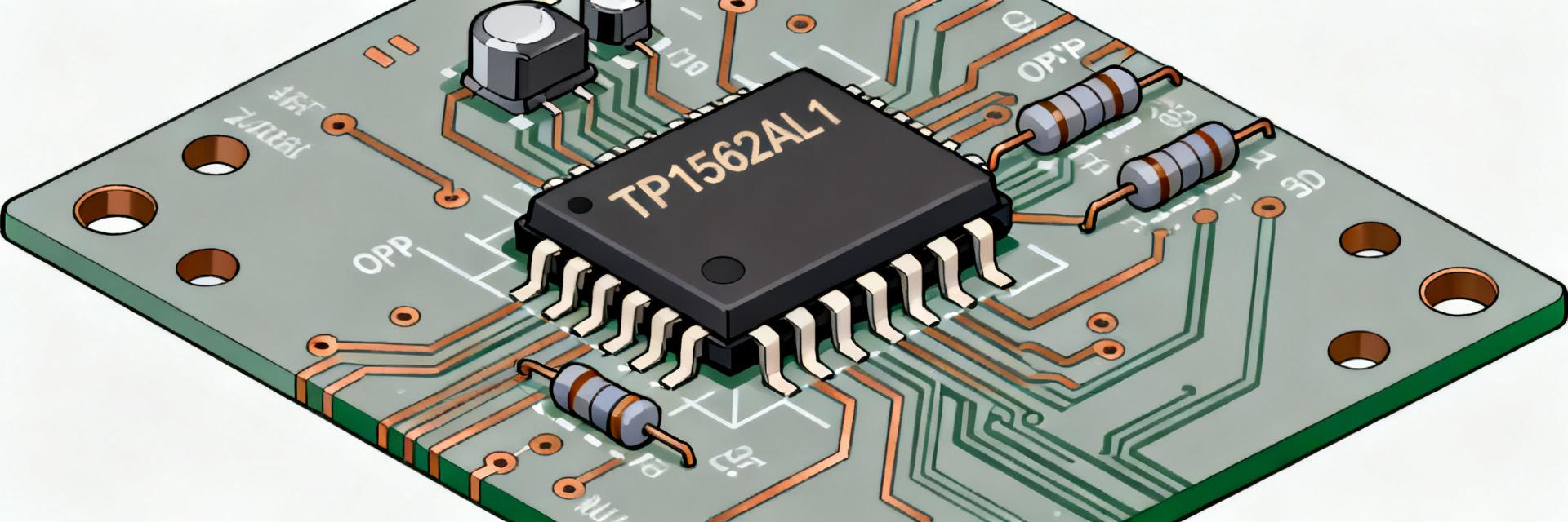
Point: The TP1562AL1 is a dual, low‑power rail‑to‑rail I/O op amp tailored for single‑supply battery and general‑purpose applications. Evidence: Typical quiescent current is ≈600 μA per channel, supply operation spans ~2.5–6.0 V, and gain‑bandwidth sits in the single‑digit MHz range. Explanation: This brief presents a datasheet‑style quick‑spec snapshot, a condensed measured‑data summary, and recommended test guidance so engineers can validate TP1562AL1 performance under defined VCC, load, and ambient conditions.
1 — At‑a‑Glance Quick Specs (background introduction)
1.1 — What to list in the one‑page spec snapshot
Point: A one‑page spec must capture function, packages, and key electrical parameters. Evidence: Essential fields include part function (dual op amp), package options, supply range, quiescent current/channel, GBW, slew rate, rail‑to‑rail I/O note, output drive (RL), input offset and drift, input bias, CMRR, PSRR, noise, and operating temperature. Explanation: Present each value with units and explicit test conditions (VCC, gain, RL, temperature) so readers can compare guaranteed datasheet numbers vs typical bench measurements.
1.2 — SEO & reader tips for the snapshot
Point: Label the snapshot clearly for searchability and clarity. Evidence: Use headings such as "TP1562AL1 specs / TP1562AL1 datasheet" and add a one‑line "typical vs guaranteed" callout. Explanation: That callout helps engineers know which entries are expected typical lab results and which are guaranteed by the supplier for design margin and compliance.
| Parameter | Typical / Condition |
|---|---|
| Function | Dual operational amplifier |
| Package | SOP, WSON variants (verify ordering code) |
| Supply V | 2.5–6.0 V (single supply) |
| Quiescent Current | ≈600 μA/channel (VCC=5 V, no load) |
| GBW | ~5–9 MHz typical (gain = 1) |
| Slew Rate | ~3–6 V/μs typical (RL≥2 kΩ) |
| Rail‑to‑rail I/O | Yes (within ~100 mV of rails into light RL) |
| Output Drive | ±10 mA into 2 kΩ |
| Input Offset | ~0.5–3 mV typical |
| Input Bias | nA range typical |
| CMRR / PSRR | ~70–100 dB typical (low freq) |
| Noise | nV/√Hz range (specify bandwidth) |
| Operating Temp | -40 to +85 °C |
2 — Key Electrical Characteristics (data analysis)
2.1 — Power and supply behavior
Point: Supply voltage and quiescent current dominate battery life and thermal design. Evidence: The device runs from ~2.5 to 6.0 V; quiescent current climbs slightly with VCC and temperature (typical ~600 μA/channel at 5 V). Explanation: For battery applications pick the lowest acceptable VCC to minimize Iq, verify idle and active currents across temp corners, and compute power dissipation (P ≈ VCC × Iq × channels) to assess thermal stress on small PCBs and coin‑cell scenarios.
2.2 — Input/output and dynamic specifications
Point: Dynamic figures determine suitability for ADC drivers and sensor front ends. Evidence: Input common‑mode includes both rails; output swing approaches rails into light loads; GBW in single‑digit MHz and slew ~a few V/μs. Explanation: Replicate datasheet conditions when measuring: unity gain for GBW, specified RL for output swing, and defined gain for small‑signal bandwidth. Note offset and bias current impact on precision DC paths and source impedance.
3 — Measured Bench Results Summary (data analysis / case)
3.1 — What measured tests to include and expected ranges
Point: Publish measured quiescent current, GBW, slew, offset, PSRR/CMRR, output swing, THD/noise. Evidence: Typical measured ranges: Iq ≈600 μA/channel (VCC=5 V), GBW ~5–9 MHz, slew ~3–6 V/μs, offset ~0.5–3 mV. Explanation: For each test state conditions (VCC, RL, gain, temperature) and include the datasheet guarantee line so readers can see deltas between guaranteed and typical lab values.
3.2 — Example measured summary table layout
| Test | Condition | Datasheet | Measured | Delta | Notes |
|---|---|---|---|---|---|
| Quiescent Current | VCC=5 V, no load, 25 °C | ≤X μA | ~600 μA | typical | Channel A/B averaged |
| GBW | Gain=1, VCC=5 V | Y MHz | 5–9 MHz | ±Z% | Bode plot recommended |
| Slew Rate | Large step, RL=2 kΩ | S V/μs | 3–6 V/μs | — | Measure rising/falling |
Explanation: Add oscilloscope thumbnails or Bode plot thumbnails tied to these table rows for reproducible reporting.
4 — Recommended Test Methods & Fixtures (method guide)
4.1 — Equipment checklist & measurement setup
Point: Proper instruments and fixture minimize measurement error. Evidence: Required tools include a low‑noise DC supply, precision meter, function generator, oscilloscope with compensated probes, and network or spectrum analyzer for GBW/THD. Explanation: Use a compact PCB with solid ground plane, close decoupling (0.1 μF + 10 μF), short traces, and proper probe grounding to avoid ringing and false noise readings.
4.2 — Step‑by‑step procedures for critical tests
Point: Follow consistent procedures for Iq, GBW, slew, PSRR/CMRR, and output swing. Evidence: Examples — Iq: measure supply current with outputs in midrail, no load; GBW: configure as buffer, sweep with network analyzer; slew: apply a 5 Vpp step and measure slope into RL. Explanation: Record checkpoints: VCC, ambient temp, gain, RL, and probe type; log raw CSVs and waveform images for traceability.
5 — Application Examples & Selection Checklist (action recommendations)
5.1 — Typical application scenarios
Point: Two representative uses illustrate tradeoffs. Evidence: Use case A — low‑power sensor front end on a single 3.3 V battery rail (prioritize Iq and offset). Use case B — ADC buffer for microcontroller input at 5 V (prioritize rail‑to‑rail swing and GBW). Explanation: For each case state recommended VCC, expected bandwidth and slew requirements, and focus tests: Iq/offest for A; output swing, THD and small‑signal bandwidth for B.
5.2 — Selection and layout checklist with common pitfalls
Point: Layout and test artifacts often cause discrepancies. Evidence: Checklist items include decoupling close to pins, avoid long input traces, limit capacitive loads or add isolation resistor, verify probe compensation, and confirm RL meets output drive specs. Explanation: Quick fixes: add 50–200 Ω series resistor for stability into capacitive loads; use star ground for sensitive inputs; re‑measure after probe optimization to eliminate false noise or oscillation.
Summary
Point: The TP1562AL1 delivers low‑power rail‑to‑rail I/O with single‑digit‑MHz dynamics suitable for battery and single‑supply systems. Evidence: Typical Iq ≈600 μA/channel, VCC range ~2.5–6.0 V, and GBW and slew adequate for ADC buffering and sensor front ends. Explanation: This concise TP1562AL1 datasheet specs summary plus measured table and test methods supports reproducible validation—focus on power vs dynamic tradeoffs and report tables plus waveforms for engineering decisions.
Key Summary
- Low power and rails: TP1562AL1 typical quiescent ~600 μA/channel; suitable for battery‑powered front ends when run at the lowest acceptable VCC and monitored across temperature.
- Dynamic envelope: Expect single‑digit MHz GBW and a few V/μs slew; validate with unity‑gain Bode plots and large‑step slew tests into defined RL.
- Measurement discipline: Always log VCC, gain, RL, and ambient temp; provide CSVs and waveform thumbnails alongside the measured summary table for reproducibility.
Common Questions
What are the typical quiescent current specs for TP1562AL1 and how should they be measured?
Measure Iq per channel with outputs unloaded and biased midrail using a precision DC meter; note VCC and temperature. Typical lab results show ≈600 μA/channel at 5 V. Compare to guaranteed datasheet limits and report delta with measurement conditions (VCC, temp, channel).
How to verify TP1562AL1 GBW and slew rate for ADC buffering?
Configure the amplifier as a buffer (gain = 1), use a network analyzer or swept sine source to capture the Bode plot for GBW. For slew rate, apply a large step (e.g., 2–4 V) and measure dV/dt with an oscilloscope into the target RL; record both rising and falling edges.
Which layout and test pitfalls most commonly affect measured specs for TP1562AL1?
Common issues are poor decoupling, long input/probe leads, and capacitive loading causing instability or apparent noise. Fixes include close 0.1 μF decoupling, short ground returns, series output resistors for capacitive loads, and verified probe compensation before measurement.


