
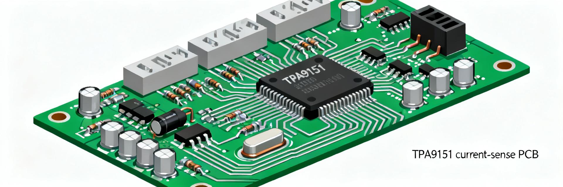
Current-sensing Circuit Report: TPA9151-SO1R Data Guide
Point: Precision telemetry and tighter control in BMS, motor drives, and power supplies are increasing the demand for accurate current measurement; this report analyzes the TPA9151-SO1R as a practical difference-amplifier building block.
Evidence: Designers increasingly require millivolt-level shunt measurements to drive ADCs and control loops.
Explanation: The TPA9151-SO1R’s trimmed resistors and reference options make it a strong candidate for low-offset, high-CMRR topologies in a modern current-sensing circuit.
Point: This guide translates datasheet language into design rules, test recipes, and an implementation checklist.
Evidence: Readers will get datasheet-to-system mappings, recommended bench setups, and production-test criteria.
Explanation: By following the scope (datasheet translation, design rules, test setup, implementation checklist) you will be able to select shunt values, set amplifier gain, and validate performance reproducibly using the TPA9151-SO1R.
1 — Background: Current-sensing circuit fundamentals & where TPA9151-SO1R fits
1 — Common topologies and trade-offs
Point: Shunt-based measurement is the dominant approach, implemented as low-side or high-side sensing, each with trade-offs. Evidence: Low-side places the sense resistor at ground for simpler common-mode but may lose isolation; high-side preserves ground reference but requires wider common-mode handling. Explanation: Choose difference amplifiers for wide common-mode ranges and instrumentation amplifiers when extremely high gain and lower offset are required, balancing accuracy, isolation, and dynamic range.
2 — Role of precision difference amplifiers in current-sensing circuits
Point: A precision difference amplifier reduces error sources by matching resistor ratios and offering reference pins for level shifting. Evidence: On-chip trimmed resistor ratios and REFA/REFB style reference capability reduce gain error and permit output offset control. Explanation: The TPA9151-SO1R’s integrated trimming and reference functionality directly addresses CMRR, offset, and gain stability constraints common in demanding applications.
2 — Datasheet deep-dive: TPA9151-SO1R electrical characteristics explained
1 — Key electrical parameters to extract and verify
Point: Identify input common-mode range, gain accuracy, CMRR vs frequency, offset and drift, bandwidth, supply limits, output swing and noise from the datasheet. Evidence: Each spec sets a system-level limit—e.g., common-mode headroom defines maximum measurable shunt placement; output swing limits ADC interfacing. Explanation: Translate specs into requirements like maximum shunt voltage, required amplifier gain to use ADC full-scale, and acceptable noise floor for your measurement resolution.
2 — Transfer function, internal resistor trimming & reference pins
Point: Understand the device transfer function including how reference pins shift the output and how on-chip resistor ratios determine gain. Evidence: The amplifier’s transfer can be represented as Vout = Gain*(V+ - V-) + Vref when REFA/REFB is used. Explanation: On the bench, confirm transfer by applying known differential inputs and Vref levels, document the measured Gain and offset, and note resistor ratio tolerance effects on absolute gain error.
3 — Design guidelines: building reliable current-sensing circuits with TPA9151-SO1R
1 — Circuit topologies, shunt selection and resistor sizing
Point: Choose a shunt value that yields measurable voltage without excessive power loss: Vshunt = I × Rshunt. Evidence: Pick Rshunt to produce a few tens to a few hundred millivolts at peak current so ADC resolution is usable but dissipation is manageable. Explanation: Calculate amplifier gain so Vout = Gain*(V+ - V-) + Vref uses ADC full-scale (e.g., 3.3 V) without saturating; include power and thermal derating for continuous current.
2 — Layout, filtering, protection and stability practices
Point: PCB layout and input protection materially affect accuracy and noise. Evidence: Short Kelvin traces, differential symmetry, and star grounds reduce common-mode and offset errors; input series resistors and RC filters limit noise and protect inputs. Explanation: Add TVS or clamp protection for transients, verify stability with capacitive ADC loads, and plan calibration strategies (offset trimming, temperature compensation) in firmware and test flows.
4 — Measurement setups and data-driven validation
5 — Implementation checklist & application examples
1 — Integration checklist for production designs
Point: Follow a concise production checklist covering schematic, PCB, BOM, test and firmware. Evidence: Key items include confirming common-mode headroom, verifying gain tolerance, specifying shunt thermal rating, and defining production-test acceptance ranges for offset and gain. Explanation: Embed calibration routines in firmware, include test points for factory verification, and set clear PASS/FAIL limits for automated production checks.
2 — Example application briefs and optimization tips
Point: Application constraints drive optimization priorities: motor drives need transient bandwidth, BMS emphasizes low drift, supplies balance bandwidth vs filtering. Evidence: For motor current sensing prioritize wide bandwidth and clamp protection; for BMS prioritize offset and temperature stability. Explanation: For each case, list top verification checks—transient response for motors, drift and noise for batteries, and filter trade-offs for supplies.
Summary
- Translate datasheet specs into system limits: extract common-mode range, gain accuracy, offset/drift, and bandwidth to size shunt and set amplifier gain for your ADC and control loop; TPA9151-SO1R’s trimmed ratios simplify this translation.
- Follow rigorous layout, filtering and protection practices: short Kelvin traces, differential symmetry, input RC filtering and transient protection reduce error sources and protect the amplifier in field conditions.
- Validate with a reproducible test plan: use DC, step and frequency tests to record gain error, offset, CMRR vs frequency and noise; document measured vs datasheet values to close design risks for any current-sensing circuit.
6 — FAQ
What common-mode range should I expect when designing a current-sensing circuit with TPA9151-SO1R?
Point: You should ensure headroom beyond the expected shunt node voltages. Evidence: Practical designs place the amplifier’s allowed common-mode a few volts above and below rails depending on supply; exceeding that causes output clipping or CMRR collapse. Explanation: Verify the datasheet common-mode window on the bench and choose shunt placement (low- vs high-side) or level-shifting so you remain within that range under all conditions.
How do I pick shunt resistance and amplifier gain for a production current-sensing circuit?
Point: Target measurable shunt voltage of tens to a few hundred millivolts at peak current and use amplifier gain to map that to ADC full-scale. Evidence: Vshunt = I × Rshunt and Vout = Gain*(V+ - V-) + Vref. Explanation: Compute Rshunt for acceptable power dissipation, then set Gain = (ADC_FSR - margin) / Vshunt, leaving headroom to avoid saturation during transients.
What are quick verification steps if measured offset or CMRR look worse than datasheet for the TPA9151-SO1R?
Point: Investigate layout, protection clamps, and thermal coupling first. Evidence: Asymmetric routing or long input traces and input clamping can introduce differential errors and degrade CMRR. Explanation: Simplify the board to a short Kelvin connection to the shunt, remove clamps temporarily to test raw behavior, and perform thermal isolation to identify the dominant error source before corrective changes.


