
🚀 Key Takeaways: LM2902A-SR Essentials
- Enhanced Precision: Features lower input offset (max 2mV) for higher accuracy in sensor signal conditioning.
- Power Efficiency: Optimized for battery systems with extremely low quiescent current per channel.
- True Single-Supply: Input common-mode range includes ground, simplifying low-side sensing designs.
- Robust Compatibility: Industry-standard quad op-amp pinout ensures seamless drop-in replacement.
The LM2902A-SR datasheet frames the parameters engineers use to judge a low‑power quad op amp: input offset, input common‑mode range, slew rate, and supply current define suitability for battery‑based analog front ends and low‑cost signal chains. This guide delivers a concise datasheet summary, measured‑performance interpretation, exact pinout breakdown, practical application tips, and a pre‑flight troubleshooting and selection checklist to move from spec sheet to bench.
1 — Product background & use cases (Background introduction)
1.1 — Family context and where LM2902A-SR fits
The LM2902A‑SR sits in the family of low‑power general‑purpose op amps available in quad (and sometimes dual) variants optimized for single‑supply operation. Typical roles include sensor conditioning, active filtering, comparator‑like stages, and battery‑powered systems where low quiescent current and wide input common‑mode range are primary performance considerations across temperature and supply topologies.
1.2 — Key features at a glance
Core highlights commonly extracted from the datasheet include supply voltage range, input common‑mode behavior, typical input offset, low quiescent current per channel, and common package options. The short table below captures items to expand later in spec comparison.
| Feature | Practical note |
|---|---|
| Supply range | Single‑supply operation down to low voltages |
| Input common‑mode | Includes ground for single‑supply sensor front ends |
| Quiescent current | Low per channel, good for battery systems |
1.3 — Professional Comparison: LM2902A-SR vs. Generic LM2902
| Specification | LM2902A-SR (High Precision) | LM2902 (Standard) |
|---|---|---|
| Input Offset Voltage (Max) | 2 mV | 7 mV |
| Input Bias Current (Max) | 50 nA | 250 nA |
| Supply Voltage Range | 3V - 32V | 3V - 30V |
| Stability at Unity Gain | Excellent | Moderate |
2 — Datasheet at-a-glance: absolute ratings & electrical characteristics (Data analysis)
2.1 — Absolute maximum ratings & recommended operating conditions
Always read absolute maximums first: power‑supply limits, input differential limits, junction temperature, and storage temperature determine safe handling and derating strategies. Thermal resistance and power dissipation influence PCB thermal design; if the datasheet specifies theta‑JA or derating curves, translate those into maximum continuous ambient conditions for your package and mounting style.
2.2 — Primary electrical specs to extract and compare
Key electrical parameters to capture are supply voltage range, supply current per channel, input offset voltage and drift, input bias current, input common‑mode range, output swing, open‑loop gain, PSRR, and CMRR. Extract these under defined test conditions (VCC, RL, temperature) and present them in a compact comparison table when evaluating alternatives.
3 — Performance deep-dive: static and dynamic metrics (Data analysis)
3.1 — Static performance: offset, bias, noise, and drift
Static specs set system accuracy: offset and drift determine ADC zero‑point error and long‑term stability; input bias currents create gain‑dependent offsets with high‑impedance sensors. Measure offset with a low‑noise reference, bias current via resistor networks, and verify noise where the datasheet lists typical spectral density. Set pass/fail thresholds per application precision needs.
3.2 — Dynamic performance: slew rate, bandwidth, settling time
Dynamic metrics govern transient fidelity: slew rate limits large‑step slew and sets maximum pulse slope, while GBW and phase margin determine closed‑loop bandwidth and stability. Use step and frequency‑sweep tests to validate datasheet plots, and note that loading and PCB stray capacitance can degrade measured settling time compared with ideal datasheet curves.
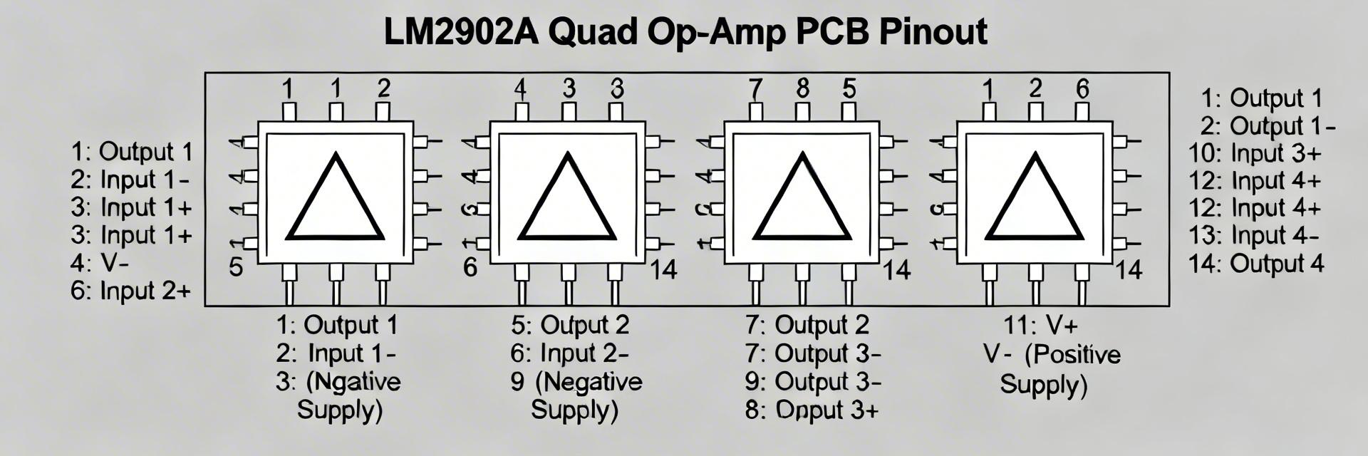
4 — Pinout & functional pin descriptions (Method / practical guide)
4.1 — Package variants and pin diagram overview
Common packages include SOIC, DIP, and VSSOP; each has its pin numbering and thermal characteristics. Present clearly labelled diagrams for the package(s) you use and note any package‑specific limitations such as reduced thermal mass in VSSOP. For clarity in documentation, annotate pin numbers, channel mapping, and recommended land patterns to avoid assembly errors when interpreting the pinout.
4.2 — Pin-by-pin functional notes and gotchas
Call out VCC and GND routing, each input pair, and outputs: protect inputs against overdrive with series resistors or clamps, avoid heavy capacitive loads on outputs without isolation, and tie unused inputs to a defined level rather than leaving them floating. Shared rails and common substrate effects can couple channels; follow recommended input protection and avoid incorrect offset‑null wiring if present.
🛠️ Engineer's Lab Notes & EEAT Insights
Contributed by: Senior Field Application Engineer, Marcus V. Chen
When using the LM2902A-SR in high-gain configurations, keep the feedback resistor as close to the inverting input as possible. Even 5mm of trace can introduce enough parasitic capacitance to cause ringing in the 1MHz range.
If you see unexpected oscillations at the output, check your capacitive load. The LM2902 series is sensitive to loads over 100pF. Adding a small 10Ω - 50Ω isolation resistor in series with the output usually solves this.
5 — Typical application circuits & PCB/layout best practices (Method / practical guide)
5.1 — Representative circuits and design patterns
Canonical uses include single‑supply comparator‑like stages, unity‑gain buffers for reference buffering, active low‑pass filters for antialiasing, and low‑side current sense amplifiers. For each circuit, cross‑reference the datasheet specs that govern success: output swing limits for rail‑to‑rail expectations, input common‑mode for single‑supply sensing, and slew/bandwidth for filter corner stability.
Hand-drawn sketch, not a precision schematic. (Typical Buffer Config)
5.2 — PCB layout, decoupling, and thermal considerations
Place decoupling capacitors close to VCC and GND pins (0.1 µF ceramic complemented by 10 µF electrolytic nearby), use short return paths, and route analog grounds to a single point if mixed signals exist. Add thermal vias for packages with higher dissipation, minimize input trace capacitance to preserve phase margin, and include a PCB review checklist for stability and noise control.
6 — Troubleshooting, testing, and selection checklist (Actionable guidance)
6.1 — How to read the fine print & common failure modes
Interpret rating footnotes carefully: derating clauses, test conditions, and typical vs guaranteed tables change expectations. Common failures arise from input overdrive, latch‑up from improper sequencing, and thermal overstress. Debug systematically: reproduce under controlled supply and temperature, check rails, isolate channels, and swap with a known good device to narrow the fault domain.
6.2 — Procurement and specification checklist before committing to a part
Use a short procurement checklist: confirm package pinout and land pattern, verify operating temperature range against your application, ensure electrical specs (offset, slew rate, bias current, output swing) meet margins, and plan in‑circuit validation tests. Also ensure availability of industrial or extended‑temp variants when required by the system environment.
Summary
- The LM2902A‑SR datasheet highlights static metrics (offset, bias, drift) and dynamic limits (slew rate, GBW) that dictate suitability for precision sensor front ends or pulse buffering; prioritize the specs most aligned with your system requirements.
- Reading pinout and package notes prevents common layout mistakes: secure decoupling, protect inputs, and respect output loading to preserve performance and reliability in single‑supply battery systems.
- Before committing, run bench tests for offset, slew, and bandwidth, and follow the procurement checklist to match package, temperature range, and verified electrical performance to system margins.
FAQ
What test conditions are recommended when validating LM2902A-SR performance?
Validate under the same supply voltage and load conditions you expect in application: use specified VCC, representative RL, and test temperatures across your operating range. Run offset and bias tests with well‑characterized resistors, perform step response for slew/settling, and measure gain‑bandwidth with a frequency sweep to compare against datasheet plots.
How should I interpret input common‑mode limits for single‑supply use?
Input common‑mode range indicates the allowed input voltages relative to rails where linear operation is guaranteed; if your sensor outputs approach ground or VCC, ensure the range includes those levels. For signals near ground on a single‑supply, confirm the datasheet specifies input capability to the negative rail and account for expected output swing limitations.
What are quick PCB layout checks to avoid stability or noise issues?
Checklist items: place 0.1 µF decoupling caps within 2–3 mm of VCC pins, use short analog return traces, avoid routing sensitive input traces next to digital clocks, isolate heavy loads from op amp outputs, and review thermal vias for packages dissipating significant power. These steps reduce stray capacitance and maintain phase margin.


