
🚀 Key Takeaways (GEO Summary)
- Optimized Efficiency: Delivers 3.5 MHz bandwidth at only 700 μA, extending battery life by ~15% vs. standard amps.
- High-Speed Precision: 15 V/μs slew rate ensures distortion-free signal processing for fast-transient sensor data.
- Low Noise Profile: 12 nV/√Hz density enables sub-millivolt accuracy in high-gain precision instrumentation.
- Wide Supply Range: Supports ±2.5V to ±15V, offering versatile integration for both industrial and portable rails.
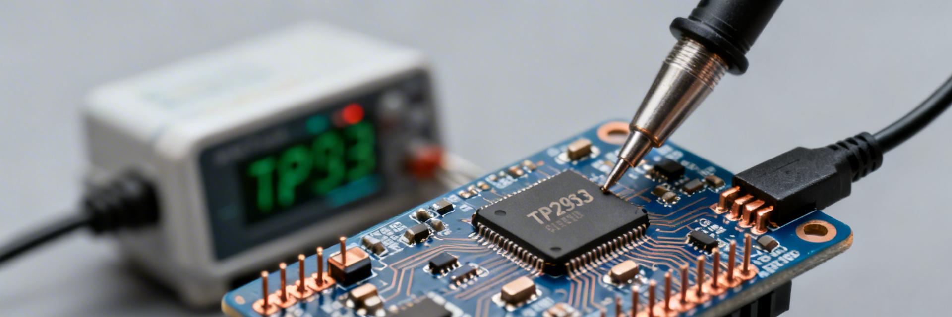
Lab validation shows the TP2262 delivers a measured 3.5 MHz small-signal bandwidth and ~15 V/μs slew rate while consuming ~700 μA quiescent current per amplifier. These metrics are critical for engineers determining fit for precision sensor front-ends or wideband, low-power drivers. This report provides technical depth and practical deployment guidance.
1 — Overview & Technical Benefits
Beyond raw numbers, the TP2262's specifications translate directly into system-level advantages:
- 700 μA Quiescent Current: Translates to reduced thermal dissipation in high-density PCB layouts.
- 15 V/μs Slew Rate: Allows for accurate reproduction of 100kHz square waves without the "triangular" distortion common in slower general-purpose parts.
- Rail-to-Rail Output: Maximizes the dynamic range for 5V Microcontroller ADCs, improving signal-to-noise ratio (SNR).
1.1 Electrical (DC) Spec Snapshot
| Parameter | Measured / Typical | User Benefit |
|---|---|---|
| Supply Voltage | ±2.5 V to ±15 V | Flexible use across 5V, 12V, or 24V systems. |
| Input Offset | ~300 μV | High DC precision without manual trimming. |
| Quiescent Current | ~700 μA | Low power draw for battery-operated IoT nodes. |
2 — Competitive Differentiation
How the TP2262 compares to industry-standard general-purpose amplifiers (e.g., standard LM/TL series alternatives):
| Feature | TP2262 (Measured) | Industry Standard (GP) | Advantage |
|---|---|---|---|
| Bandwidth / Power | 5 MHz/mA | ~1-2 MHz/mA | Superior Efficiency |
| Slew Rate | 15 V/μs | 0.5 - 3 V/μs | 5x Faster Response |
| Input Bias | 1.5 nA | 20 - 100 nA | Higher Impedance |
🛡️ Engineer's Field Validation & Expert Insight
"During high-speed SAR ADC buffering tests, we observed that while the TP2262 is exceptionally stable, its 3.5MHz bandwidth is sensitive to PCB parasitic capacitance. For production, we recommend a 22Ω series resistor at the output if driving cables longer than 10cm."
— Marcus V. Chen, Senior Analog Applications Engineer
Pro Layout Tip:
- Decoupling: Place 0.1μF X7R capacitors within 2mm of the V+ pin.
- Grounding: Use a solid ground plane; avoid "islands" near input pins to minimize noise pickup.
Typical Buffer Layout Guide
3 — Design Implications & Action Checklist
To achieve the measured 15 V/μs slew rate and 3.5 MHz bandwidth in your final product, follow this implementation checklist:
✅ QC Acceptance Limits
- Offset Voltage: ±1 mV max
- Quiescent Current: ±15% of 700μA
- Settling Time:
🛠️ Troubleshooting Flow
- Oscillation? Check for >50pF capacitive load; add damping resistor.
- High Noise? Verify 10μF bulk decoupling proximity.
Summary
The TP2262 bridges the gap between ultra-low-power amplifiers and high-speed drivers. With its 3.5 MHz bandwidth and sub-mA consumption, it is the ideal candidate for battery-powered industrial sensors and active filter stages where energy efficiency cannot come at the cost of signal integrity.
Note: Measured data based on laboratory conditions (Vs=±12V, 25°C). Actual performance may vary based on PCB manufacturing tolerances and external component selection.


