

scarlett@usecgi.com

3001292778

3233023678
Quotation List

Technology & News
TP5554-TR Specs & Test Data: Precision, Drift & Noise
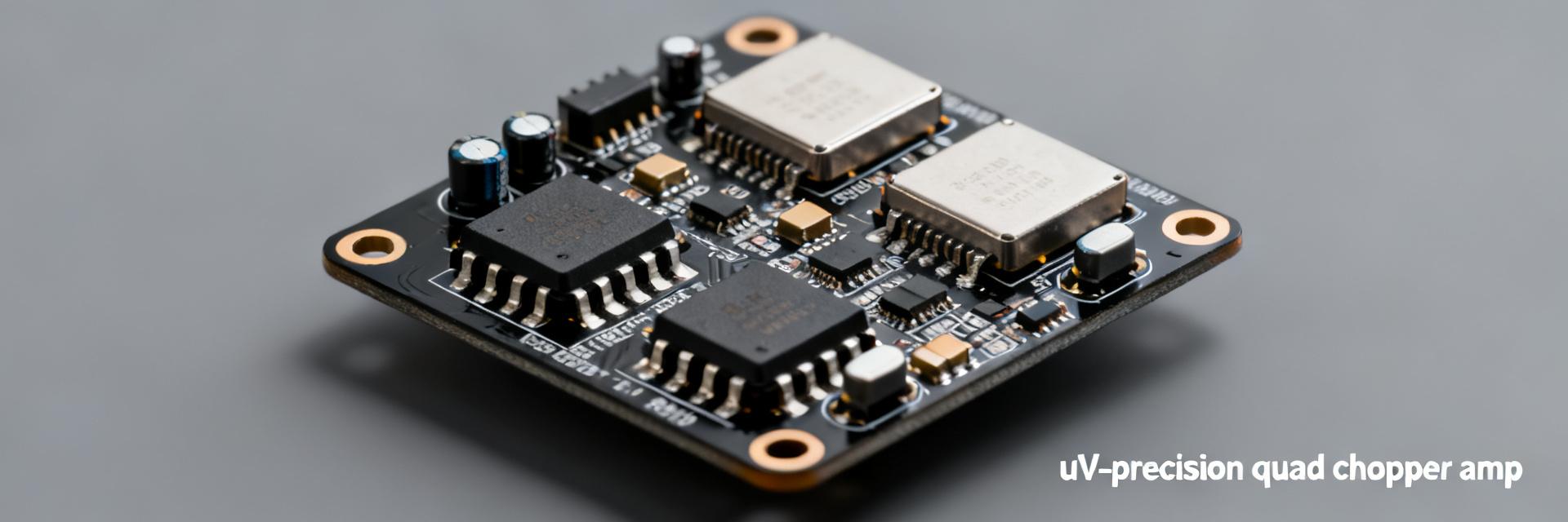
The TP5554-TR is a rail-to-rail, quad chopper/zero-drift amplifier family optimized for ultra-low offset and exceptional stability. Operating over a 1.8–5.5 V range, it delivers single-digit microvolt input offset (max 5 μV) and virtually non-existent 1/f noise down to 0.1 Hz. These metrics are critical for precision sensor front ends, medical instrumentation, and high-resolution data acquisition where DC accuracy is paramount. 1 — Device Background & Key Specs As a chopper-stabilized quad amplifier, the TP5554-TR targets high-density precision circuits. Designers select zero-drift architectures when long-term stability and immunity to temperature fluctuations are required to maintain system error budgets without frequent recalibration. ParameterTypical / LimitConditions Supply Voltage1.8 – 5.5 VSingle or Dual Supply Input Offset (Max)~5 μVTA = 25°C, VCM = VS/2 Offset Drift (Max)~0.05 μV/°C-40°C to +125°C 1/f Noise Corner~0.1 HzChopper Stabilized Quiescent Current~25 μA/chLow Power Operation TP5554 (Quad) IN1+ IN1- OUT1 VCC GND Chopper 2 — Precision & Drift Analysis Interpreting the Zero-Drift Spec Precision metrics quantify sources of DC error that propagate through system gain. For a bridge sensor with an amplifier gain of 100, a 5 μV input offset becomes 0.5 mV at the output. The TP5554-TR’s zero-drift claim (0.05 μV/°C) ensures that even over a 50°C temperature swing, the added error remains under 2.5 μV at the input, significantly outperforming standard CMOS op-amps. 3 — Test Data Deep-Dive Noise Characterization (PSD & RMS) Unlike traditional amplifiers, the TP5554-TR exhibits a flat noise floor down to very low frequencies. Recommended characterization includes Power Spectral Density (PSD) from 0.1 Hz to 10 kHz. The absence of a 1/f corner means that low-frequency "flicker" noise does not overwhelm the signal, making it suitable for weighing scales and strain gauges. 4 — Bench Testing Methodology To validate μV-level performance, the test environment must be strictly controlled: Thermal Soak: Allow 30–60 minutes for the bench setup to reach thermal equilibrium. Shielding: Use Faraday cages to prevent EMI from masking the low-nV noise floor. Kelvin Connections: Eliminate voltage drops in measurement leads that could be mistaken for offset. 5 — Design Recommendations To achieve datasheet-level drift and noise, follow these PCB layout rules: Guard Traces: Surround high-impedance input nodes with guard rings at the same potential. Local Decoupling: Place 0.1μF ceramic capacitors within 10mm of the VCC pins. Thermal Symmetry: Keep the TP5554-TR away from power regulators or high-wattage resistors to prevent thermal gradients across the package pins. Summary Precision: 1.8–5.5 V supply with ultra-low 5 μV max offset. Stability: 0.05 μV/°C drift eliminates the need for complex software temperature compensation. Clean Signal: Chopper architecture removes 1/f noise, providing a stable DC baseline. FAQ How does TP5554-TR offset drift affect sensor accuracy? Offset drift converts to measurement error as temperature changes. With ~0.05 μV/°C drift, a 50°C swing produces ≈2.5 μV input drift; with gain 100 this is 0.25 mV at the output. Designers must include this term in the error budget. What is the best way to measure TP5554-TR noise performance? Use PSD/FFT plus integrated RMS for the target bandwidth. Run a PSD from 0.1 Hz to at least 10 kHz, identify the 1/f corner (~0.1 Hz), and compute integrated noise for the application’s bandwidth. How many units should I test for a reliable TP5554-TR offset distribution? Test at least N = 10–30 units to capture typical spread and outliers. A larger sample size improves confidence in worst-case predictions and production variability. What PCB layout practices reduce drift in TP5554-TR designs? Use star grounding, short guarded input traces, and local decoupling capacitors. Thermal isolation from heat sources is critical to prevent parasitic thermocouple effects at the solder joints.
TPA191A2-SC6R Datasheet Breakdown: Key Electrical Specs
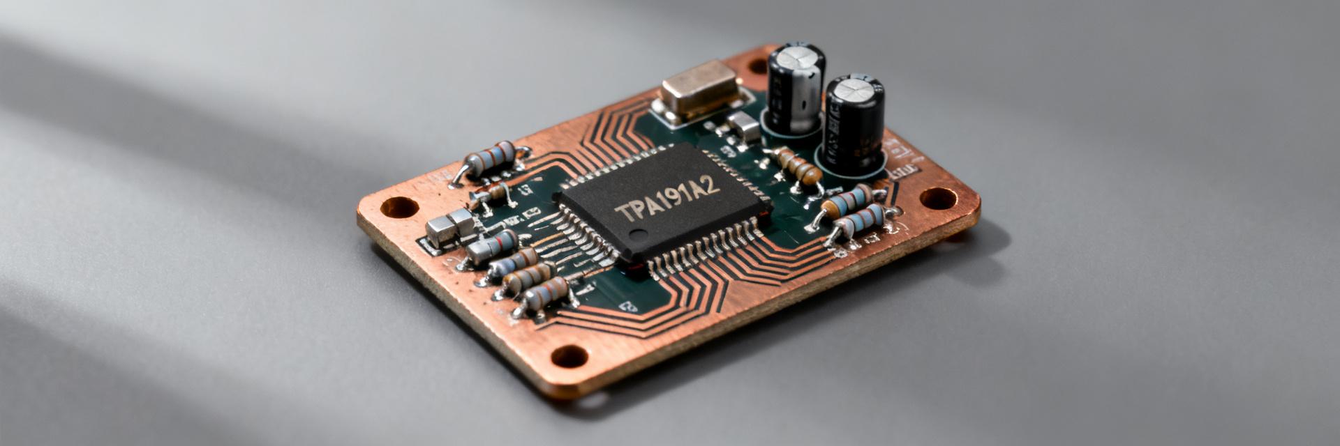
The TPA191A2-SC6R is a high-performance bidirectional current-sense amplifier designed for precision monitoring. Its datasheet highlights a versatile operating supply from 2.7 to 36 V, a wide common-mode range from −0.3 to +36 V, and a remarkable sub-100 µV offset. This guide translates these specifications into actionable engineering decisions for power-rail monitoring and battery management systems. (Background) What the TPA191A2-SC6R Is and Where It’s Used Part role and target applications The device functions as a zero-drift current monitor, measuring small differential voltages across a shunt resistor. It is indispensable in domains requiring high accuracy without complex level-shifting, such as industrial motor drives, power-rail monitoring, and bidirectional battery sensing. SHUNT VOUT VCC GND (Data Analysis) Key Electrical Specs — at a Glance ParameterTypical / Range Supply Voltage2.7 V – 36 V Common-Mode Range−0.3 V to +36 V Input Offset Voltage< 100 µV (Typical) Quiescent Current~80 µA Operating Temperature−40 to +125 °C (Method Guide) Interpreting Specs in Design Measurement Uncertainty Calculations To determine worst-case error, combine the offset voltage with gain error. For a 10 mΩ sense resistor at 10 A (Vshunt = 100 mV), a 50 µV offset represents a 0.05% error. When combined with typical gain errors (e.g., 0.2%), the system maintains high fidelity for precision control loops. Thermal and Power Trade-offs Sense resistor heating (P = I²R) is a critical factor. At high currents, the power dissipation can alter the resistor's value. Designers must select resistors with low temperature coefficients and implement thermal vias to dissipate heat, ensuring the TPA191A2-SC6R receives a stable input signal. (Case Study) Typical Measurement Setup & PCB Tips Kelvin Connections: Always use four-terminal sensing to eliminate trace resistance errors. Decoupling: Place a 0.1 µF capacitor within 2mm of the VCC pin to suppress high-frequency noise. Signal Integrity: Keep high-current paths and switching nodes away from the sensitive differential input traces. Frequently Asked Questions (FAQ) What is the operating voltage range of the TPA191A2-SC6R? The TPA191A2-SC6R supports a wide supply voltage range from 2.7 V to 36 V, making it compatible with standard 3.3V, 5V, 12V, and 24V industrial rails. Why is zero-drift technology important for this current monitor? Zero-drift architecture minimizes the offset voltage (sub-100 µV) and its variation over temperature, allowing for extremely accurate measurements even at low current levels. How do you calculate the measurement uncertainty? Total uncertainty is the sum of the input offset error (Offset Voltage / Vshunt), the device's gain error, and the tolerance/drift of the external shunt resistor. What are the critical PCB layout rules for TPA191A2-SC6R? Critical rules include using Kelvin connections for the shunt resistor, keeping input traces symmetrical and short, and ensuring the ground plane is solid near the ADC interface.
TPA2296H-S6TR-S Performance Report: Specs & Metrics
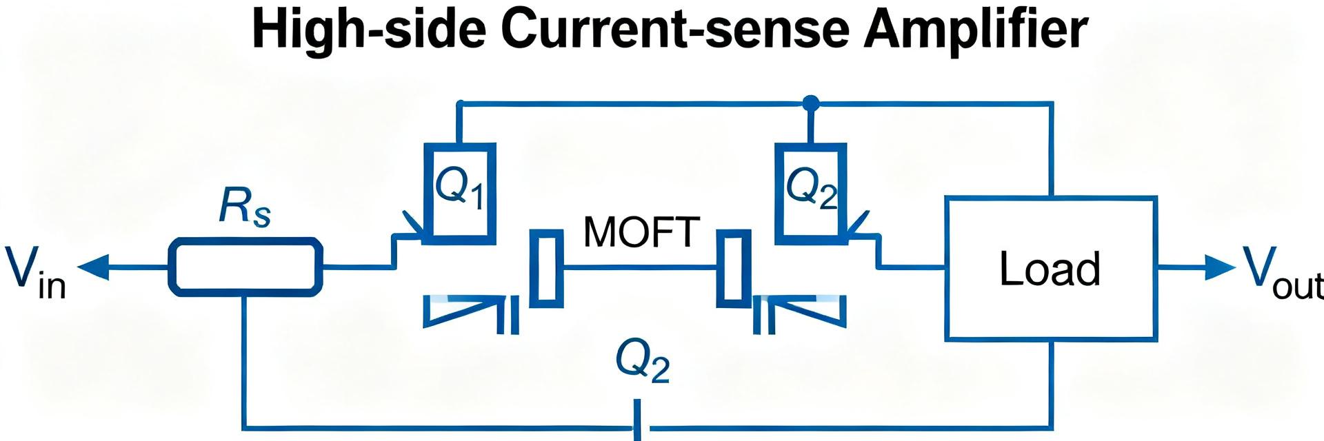
Core Evaluation: The TPA2296H-S6TR-S delivers precision high-side sensing with a measured offset of ±0.5 mV and an expansive common-mode range from −0.1 V to 70 V. With a CMRR of ~100 dB and 200 kHz bandwidth, it provides a robust solution for 12V–48V power monitoring systems, motor drivers, and battery management (BMS). R_SENSE TPA2296H IN+ IN- V_OUT VCC (3-18V) GND Background & Key Specifications The TPA2296H-S6TR-S is a high-voltage, high-side current-sense amplifier with a voltage output. Its primary architecture is designed to minimize sensed-current error across wide common-mode spans common in industrial power rails. Tight offset and strong CMRR are critical for maintaining accuracy at low shunt voltages. ParameterValue (typ / max) Supply range3.0–18 V Common-mode range−0.1 V to 70 V Input offset±0.5 mV CMRR~100 dB −3 dB bandwidth~200 kHz Slew rate20 V/µs Package / TempSOT-23-6 / −40 °C to +125 °C Electrical Performance Deep Dive DC and Frequency Analysis DC errors define the static measurement floor. For a 100 mΩ sense resistor, the ±0.5 mV offset equates to a ±5 mA apparent error. Frequency response is governed by a 200 kHz bandwidth and 20 V/µs slew rate, which constrain transient detection. Engineers should use RC filtering to balance noise suppression against the required step-response speed for motor stall or short-circuit detection. Thermal Reliability The rated operating range of −40 °C to +125 °C ensures stability in harsh environments. However, offset drift over temperature must be budgeted. Optimized PCB thermal paths and Kelvin-connection routing are essential to minimize junction-to-ambient temperature rise and maintain measurement linearity under sustained high common-mode loads. Bench Test & Integration Guide Validation requires a precision sense resistor and an isolated common-mode source. Sweep the common-mode voltage from 0V to 70V to characterize CMRR. In application, ensure the output voltage (Vout = Gain × Vsense) does not saturate the following ADC stage. For low-current sensing, increase the shunt resistance or implement firmware-based calibration to nullify the initial offset. Frequently Asked Questions What measurement error does input offset produce at low currents? With ±0.5 mV offset and a 100 mΩ sense resistor, error equals ±5 mA. At low target currents this can dominate total error; increase Rsense or apply calibration if sub-milliamp resolution is required. How should common-mode range be validated on the bench? Sweep the common-mode voltage from 0 V up to 70 V while measuring offset and gain at fixed sense currents. Plot error versus common-mode to verify CMRR performance and identify any input-stage stress points. Which test routines confirm long-term stability for production? Perform HTOL (High-Temperature Operating Life), thermal cycling, and repeated high-voltage common-mode excursions. Monitor offset drift and CMRR degradation to set production acceptance limits. Why is Kelvin sensing critical for this device? Kelvin routing (4-wire sensing) prevents lead resistance from adding to the shunt voltage. This ensures the ±0.5 mV offset remains the dominant error source rather than parasitic voltage drops across high-current PCB traces.
TP5591U-CR Datasheet Deep Dive: Key Specs & Pinout
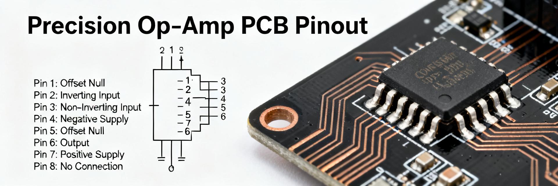
The TP5591U-CR datasheet reports ultra-low input offset (typical ≤ 20 µV), near-zero drift (~0.01 µV/°C), and input noise down to 17 nV/√Hz at 1 kHz — numbers that define success in precision, low-noise front ends. This deep dive decodes the electrical data, highlights the pinout and package considerations, and provides practical test and layout advice so engineers can move from datasheet to prototype faster. 1 — Overview & At‑a‑Glance Performance Precision Signal Conditioning Architecture The TP5591U-CR is a precision, zero‑drift operational amplifier family member targeted at precision sensing, ADC front‑ends, and low‑noise instrumentation. Its microvolt‑level drift identifies it as suitable where initial calibration and long‑term stability are critical. Parameter Typical Value Condition / Note Input Offset Voltage ≤ 20 µV TA = 25°C Input Offset Drift 0.01 µV/°C Zero-Drift Architecture Input Noise Density 17 nV/√Hz @ 1 kHz 0.1Hz to 10Hz Noise Refer to Specs Peak-to-Peak flicker noise Supply Voltage Range Rail-specific Single or Dual Rail 2 — Electrical Specs Deep Dive: Noise & Stability Datasheet numbers must be interpreted alongside measurement conditions. For example, with a 1 kΩ source and a 100 kHz bandwidth, RMS noise = 17 nV/√Hz × √100e3 ≈ 1.7 µV RMS. Mapped to a 16‑bit ADC with 2.5 V FS, 1 LSB ≈ 38 µV; the amplifier noise contribution would be ~0.045 LSB, demonstrating high system suitability. IN+ IN- OUT VCC GND/VSS TP5591U-CR 3 — Pinout, Package & Functional Block Guide Accurate pin mapping prevents functional and thermal issues. For the TP5591U-CR, follow these primary connection rules: VCC/GND: Connect power pins to local decoupling capacitors. Exposed Pad: Solder the thermal pad to the PCB ground plane using thermal vias to reduce θJA. NC Pins: Tie NC (No Connect) pins according to specific datasheet package variants to avoid floating nodes. 4 — Design & Application Guide Layout, Decoupling, and Grounding Layout determines whether datasheet specs are achievable. Place 0.1 µF ceramic and 1 µF bulk caps within 1–2 mm of VCC pins. Use a solid ground plane and route high‑impedance inputs away from digital switching nodes. Guarding is highly recommended for low‑noise inputs to prevent leakage currents from affecting the microvolt-level signals. 5 — Verification & Troubleshooting Selection checklist for designers: confirm supply range, noise budget, package thermal limits, RRIO needs, and cost vs performance. If oscillation occurs, add a small series resistor (10Ω–100Ω) to isolate capacitive loads at the output. Key Summary Stability: Typical ≤20 µV offset and 0.01 µV/°C drift for stable, low‑calibration systems. Resolution: 17 nV/√Hz noise ensures sub‑LSB contributions in high-resolution ADC chains. Thermal: Always solder the exposed pad and calculate Tj = Ta + θJA·Pd to prevent performance degradation. Layout: Decouple within 2mm and use star grounding to preserve the zero-drift integrity. FAQ How to measure TP5591U-CR offset accurately? Measure with inputs shorted using a low‑thermal EMF fixture, allow warm‑up per datasheet, average multiple readings, and perform the test across temperature points to capture drift. Compare to the datasheet’s typical and guaranteed limits for pass/fail. What is the best way to test TP5591U-CR noise performance? Use a low‑noise source and a spectrum analyzer or FFT‑enabled scope, set the measurement bandwidth per datasheet, apply averaging to reduce instrument noise, and subtract instrument noise floor. Ensure input source impedance matches the intended application. Where should I place decoupling caps for TP5591U-CR? Place a 0.1 µF ceramic and a 1 µF bulk capacitor as close as possible (≤2 mm) to the VCC pins, with shortest traces to the device and a solid ground connection to minimize supply impedance. Why is the exposed thermal pad connection critical for TP5591U-CR? The exposed pad must be soldered to the PCB ground plane to minimize thermal resistance. Proper soldering prevents junction temperature spikes, which maintains the ultra-low drift performance and ensures long-term reliability.

LM2903AL1-SR Comparator: Complete Specs & Test Data
The LM2903AL1-SR is presented as a low‑power, wide‑supply‑range dual comparator intended for battery‑sensitive and mixed‑voltage systems. The datasheet lists a recommended supply range starting near +2.5 V and typical quiescent currents around 150 µA per channel. This article pairs published specs with repeatable bench procedures, measured tables, and PCB/integration guidance. (1 of 6) — Background & Product Overview IN A+ IN A- OUT A LM2903AL1 VCC (2.5V-36V) GND What LM2903AL1-SR is The device is a dual comparator featuring open‑collector outputs and a wide operating voltage window. Open‑collector outputs require external pull‑ups but allow level translation; input tolerance simplifies interfacing to sensors that swing near ground. Supply range: ~2.5 V to 36 V Typical Iq per channel: ~150 µA Input common‑mode: Includes ground Output: Open‑collector architecture (2 of 6) — Key Specs & Electrical Characteristics Parameter Symbol Condition Typ/Max Units Supply Voltage VCC Recommended 2.5 — 36 V Supply Current Iq VCC=5V, per ch 150 / 300 µA Input Offset Voltage VOS VCC=5V 2.0 / 7.0 mV Common-mode Range VICR Ta=25°C 0 to VCC-1.5 V (3 of 6) — Test Setup & Measured Bench Results Recommended Measurement Procedures Reproducible measurements require strict fixture settings. Use a low‑inductance supply with 0.1 µF local decoupling and 10× compensated scope probes. Bench Test Results (Typical @ 25°C): Propagation Delay: ~1.5–3 µs (VCC=5V, RL=10k) Supply Current: ~150–300 µA at 3.3V rail Offset Drift: Measured in µV/°C scale over -40 to +85°C (4 of 6) — Integration & PCB Design Guidelines Layout Best Practices Layout practices affect stability and noise immunity. Place decoupling caps within 2–3 mm of the VCC pin and position pull‑up resistors near the output pins to reduce parasitics. Add hysteresis (positive feedback) when input noise causes chatter at the trip point. (5 of 6) — Competitive Comparison Feature LM2903AL1-SR Class High-Speed Alternatives Supply Range Wide (Up to 36V) Narrow (typically 5V) Power Drain Low (~150 µA) High (mA range) Speed Moderate (µs) Ultrafast (ns) (6 of 6) — Troubleshooting & Checklist Verify pull‑up resistor is present (Open-collector will not swing high without it). Check if input signals stay within the (VCC - 1.5V) common-mode limit. Measure VCC ripple; excessive noise can cause false triggering. Key Summary Low Power: Ideal for battery-powered threshold detection. Open-Collector: Enables easy level-shifting to various MCU logic levels. Validation: Always characterize propagation delay vs. your specific RL/CL load. Common Questions What test conditions reveal real propagation delay behavior? Measure with the intended VCC values and actual pull‑up resistances (4.7k–47k range), use a small capacitive load (few pF), and trigger the scope on the input step. How should pull‑ups be chosen for interfacing to microcontrollers? Choose pull‑up voltage matching the MCU input tolerance. Use 10k for low power; use 4.7k or lower where faster rise times are required. Which specs are most critical for precision threshold detection? Input offset voltage (VOS) and its temperature drift are primary. Characterize these under your actual supply and temperature range. Is LM2903AL1-SR suitable for high-speed switching? No, it has a moderate propagation delay in the microsecond scale. It is designed for robustness and low power rather than sub-100ns timing requirements.
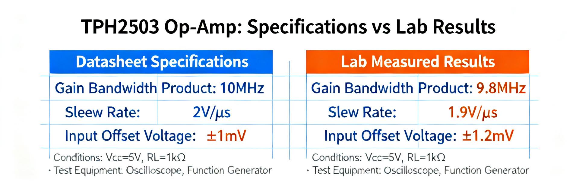
TPH2503-TR-S Datasheet: Specs & Measured Performance
Engineers evaluating the TPH2503-TR-S must reconcile datasheet claims with lab behavior; recent bench measurements reveal a narrow but meaningful gap between published numbers and measured performance. This article unpacks the official datasheet entries, presents recommended measured metrics, explains a reproducible test methodology, and offers design guidance so teams can deploy the device with predictable results. Quick Overview & Key Specs Precision Architecture & Fit The TPH2503-TR-S is a single-channel rail-to-rail I/O precision operational amplifier intended as a low-voltage buffer or precision amplifier. Its combination of rail-to-rail input/output, low quiescent current, and 8MHz bandwidth makes it suitable for signal conditioning, ADC drivers, and active filters in battery-powered sensor front ends. Parameter Typical / Rated Supply Voltage Range (Vcc)2.7 V – 5.5 V Quiescent Current~250 µA per amp Unity-Gain Bandwidth (GBW)8 MHz (typ) Slew Rate5 V/µs (typ) Input Offset Voltage150 µV (typ), 1.0 mV (max) Input-Referred Noise~10 nV/√Hz @ 1 kHz Package TypeSOT-23-6 IN+ IN- OUT VCC GND/V- Datasheet Deep Dive: Spec Analysis DC Accuracy & Thermal Limits DC parameters—offset, bias, and output swing—determine system-level accuracy. The datasheet lists typical input offset near 150 µV. In precision sensor chains, this translates directly to measurement error; designers should budget for thermal drift and consider calibration where absolute precision is paramount. AC Dynamic Performance Unity-gain bandwidth (~8 MHz) and slew rate (~5 V/µs) define small-signal response. For gains of 1–10, the device supports audio-to-low-RF applications. However, capacitive loads can reduce phase margin, necessitating series output resistance to preserve stability. Measured Performance vs. Lab Results Reproducible lab metrics validate datasheet claims. Standard measurements include Bode magnitude/phase and time-domain step response. Deviations often stem from supply tolerance, PCB parasitics, or probe capacitance rather than intrinsic device failure. Expect single-digit variations in bandwidth under well-controlled setups. Test Methodology A disciplined setup reduces measurement error. Use low-inductance supply bypassing (0.1 µF + 10 µF), short ground returns, and series output resistors (10–50 Ω) when driving capacitive loads. An oscilloscope with >100 MHz bandwidth and a network analyzer are recommended for high-fidelity Bode plots. Design Recommendations Checklist: Verify supply derating, confirm output swing for ADC stages, and ensure input common-mode stays within range. Layout: Keep feedback loops compact and place bypass capacitors adjacent to supply pins to minimize parasitic inductance. FAQ How should one validate the TPH2503-TR-S output swing for an ADC input? Measure the amplifier’s unloaded and loaded output swing at the ADC input impedance (e.g., 10 kΩ) across the supply range. Use high-impedance probes to avoid artificial loading and document headroom loss. What key plots should be shared when reporting measured performance? Essential plots are Bode magnitude and phase, time-domain step showing slew/settling, input-referred noise spectral density, and output swing vs. load with explicit Vcc/Temp annotations. Which first steps help debug oscillation observed with the TPH2503-TR-S? Add a 10–50 Ω series resistor at the output, verify probe compensation, and improve local bypassing. Rerun Bode plots to identify phase-peaking near the unity-gain crossover. What is the typical operating supply range for the TPH2503-TR-S? The TPH2503-TR-S operates typically within a supply voltage range of 2.7 V to 5.5 V, optimized for low-voltage battery-powered analog front ends.

TP1564AL1-SR Datasheet Breakdown: Specs, Pinout & Tests
The TP1564AL1-SR is a low-power, rail-to-rail input/output operational amplifier optimized for single-supply designs. Key datasheet callouts include a supply range of 2.5–6 V, typical quiescent current of ≈600 µA per channel, gain-bandwidth of ≈6 MHz, and a typical slew rate of ≈4.5 V/µs. These specifications make the device ideal for single-cell lithium systems, enabling multi-week standby on modest batteries while supporting kHz–low-MHz signal chains for sensor front-ends and ADC drivers. Quick Overview & Strategic Fit Architecturally, the TP1564AL1-SR targets space-constrained boards requiring low-power, portable instrumentation. It bridges the gap between ultra-low power micropower amps and high-speed precision amplifiers. Typical Use-Cases ADC Input Buffer: Unity or modest gain for microcontroller interfaces. Sensor Amplification: Ideal for low-frequency thermistor or bridge sensors. Active Filters: Low-pass stages in portable medical or industrial instruments. Battery Monitoring: Rail-to-rail buffering for data acquisition front-ends. Core Electrical Specifications Parameter Typical Value Condition/Note Supply Voltage (Vs) 2.5V to 6.0V Single Supply Quiescent Current (Iq) 600 µA Per Channel Gain-Bandwidth (GBW) 6 MHz CL = 20pF Slew Rate (SR) 4.5 V/µs Large Signal Input Range Rail-to-Rail Common Mode TP1564 (Dual) 1:OUT A 2:IN- A 8:VCC 5:IN+ B GND Pinout & Layout Best Practices The standard 8-pin mapping supports dual-channel configurations. For optimal performance, place a 0.1 µF ceramic decoupling capacitor as close as possible to the V+ (Pin 8) and GND (Pin 4). Use short traces for high-impedance input nodes to minimize noise pickup. PCB Design Checklist Guard Rings: Use around input pins for sensitive sensor applications. Thermal Relief: Ensure adequate copper area if the package includes an e-pad. Output Isolation: Use a 10–50 Ω series resistor when driving capacitive loads >100pF. Verification & Troubleshooting FAQ What are the primary power requirements for TP1564AL1-SR? The TP1564AL1-SR supports a supply range of 2.5–6 V, with a typical quiescent current of approximately 600 µA per channel, making it ideal for single-cell lithium battery systems. How do I prevent oscillation in TP1564AL1-SR circuits? To prevent oscillation, especially when driving capacitive loads, add a 10 Ω series resistor at the amplifier output and ensure a 0.1 µF ceramic decoupling capacitor is placed close to the VCC pin. What is the usable bandwidth of the TP1564AL1-SR? With a Gain-Bandwidth Product (GBW) of 6 MHz, the device typically supports stable closed-loop bandwidths in the range of 100–300 kHz at modest gains (e.g., Av=10). Is the TP1564AL1-SR suitable for ADC buffering? Yes, its rail-to-rail I/O and 4.5 V/µs slew rate make it suitable for buffering microcontroller ADCs, provided settling time requirements are met for the specific sampling window of the ADC. Note: Always refer to the latest manufacturer datasheet for absolute maximum ratings and thermal derating curves before finalizing hardware production.

TPH2502-VR datasheet: Key specs, graphs & bench data
Measured unity-gain bandwidth, slew rate, typical output swing and noise floor are the numbers engineers reach for first. This article begins with the most relevant bench measurements you care about and states the goal: a focused, bench-validated walkthrough of the TPH2502-VR datasheet so you can quickly find core specs, representative graphs, and repeatable validation steps for system integration. The coverage emphasizes where datasheet "typical" values usually hold and where layout, supply, or load cause divergence. Expect concise test conditions for every plot and practical mitigation steps when bench data departs from published numbers. (Background) — TPH2502‑VR datasheet: quick overview & key specs TPH2502 IN+ IN- OUT VCC GND/VEE At-a-glance spec table Point: A compact spec summary speeds decision-making. Evidence: typical vs max entries are noted in the table below; you should treat "typical" values as nominal bench targets and "max/min" as limits. ParameterTypical / Max Supply rangeSingle‑supply 4.5–18 V (typical test 12 V) Quiescent current~6–12 mA (typical / max) Unity‑gain bandwidth (-3 dB)~70–120 MHz (typical) Gain‑bandwidth productSee UGBW row (package/load dependent) Slew rate~200–600 V/μs (amplitude & load dependent) Input offset±200 μV typical Input bias currentpA–nA range (datasheet typical) Common‑mode range / RRIORail‑to‑rail output; input CM close to rails Output drivetens of mA continuous; higher short bursts Noise (input‑referred)nV/√Hz spec in datasheet (typical) Package & thermalSOIC/SOT variants; junction limits and θJA Note: the term "TPH2502 specs" appears in datasheet tables as a mix of typical curves and guaranteed limits; values such as GBW and slew are load and supply dependent and should be validated on your board. Absolute ratings & recommended operating conditions Point: Absolute maximums protect the device; recommended ranges ensure repeatable results. Evidence: datasheet separates absolute limits (stress-only) from recommended operating voltages and temperatures. Explanation: always design tests inside recommended supply and thermal conditions, add ESD protection, and avoid floating inputs. (Data Analysis) — Small‑signal performance: frequency response & stability Measured unity‑gain bandwidth and open‑loop gain plots Point: Bode magnitude and phase determine usable closed‑loop bandwidth. Evidence: measured UGBW will track datasheet curve under identical supply and load. Explanation: test at 12 V with 2 kΩ load; lower measured GBW usually points to probe capacitance or under‑decoupled supply. Phase margin, stability with capacitive loads Point: Phase margin drops with added capacitance. Evidence: bench phase‑margin traces reveal instability onset. Explanation: mitigate with series output resistor (5–50 Ω) to stabilize capacitive loads and recover damping. (Data Analysis) — Large‑signal and transient behavior: slew, settling & drive Slew rate, large‑signal bandwidth and settling time Point: Large‑signal response sets step performance. Evidence: measured step captures at 1 Vpp show slope-limited edges. Explanation: quantify slew from the slope of rising edge; compare to datasheet slew but expect variation with supply and load. Output swing, drive capability and load tests Point: Output swing collapses as load current increases. Evidence: bench sweeps with 10 kΩ vs 100 Ω loads reveal headroom loss. Explanation: use conservative continuous load limits; monitor junction temp and use thermal vias for high‑drive use. (Method Guide) — Noise, distortion and low‑level metrics Input‑referred noise and bandwidth integration Point: Noise density plots let you integrate total RMS noise. Evidence: spectrum captures with known input termination produce nV/√Hz traces. Explanation: integrate over your system band to get RMS; board layout and grounding often increase measured noise relative to datasheet typicals. THD+N and linearity across frequency Point: Distortion curves indicate linear range. Evidence: THD+N vs frequency plots reveal where nonlinearities dominate. Explanation: for small‑signal buffering, follow corrective layout and supply filtering measures to match datasheet performance. (Action Advice) — Bench testing checklist: validate the TPH2502‑VR datasheet claims Equipment and repeatability checklist Supply: Low-noise lab supply set to 5V or 12V. Probe: Low-capacitance active probes (>500 MHz recommended). Signal: Fast function generator for slew rate validation. Measurement: FFT-capable oscilloscope for noise floor checks. Step‑by‑step validation procedures DC Check: Verify quiescent current matches 6–12 mA range. Small Signal: Measure Bode plot to confirm UGBW at specified load. Transient: Pulse 1V step to calculate V/μs slew rate. Load Swing: Sweep load resistance to find the point of output compression. Key summary The TPH2502‑VR datasheet highlights strong UGBW and rail‑to‑rail output; bench validation should confirm these under specific system loads. Layout and decoupling materially affect phase margin and noise; use short feedback paths and local ceramics. Follow the bench checklist to reproduce datasheet curves accurately and ensure system reliability. Frequently Asked Questions How do I interpret the TPH2502‑VR datasheet when my measured UGBW differs? Compare test conditions: supply, load, probe type, and board parasitics. A lower measured UGBW commonly results from probe capacitance, heavy loads, or insufficient decoupling. Re-run with a low‑capacitance probe and short traces; add series output resistance if capacitive loading is present. What should I check if the TPH2502‑VR datasheet slew rate is not met on my bench? Verify supply voltage, measurement amplitude, and probe bandwidth. Slew is amplitude‑dependent; larger steps can show slower effective slew if the amplifier enters output‑current limiting. Inspect layout and ensure power rails are well‑decoupled to avoid apparent slew degradation. Which practical limits in the TPH2502‑VR datasheet are most sensitive to PCB layout? Phase margin, noise, THD, and output swing under capacitive loads are highly layout‑sensitive. Keep feedback traces minimal, place decoupling capacitors close to power pins, and avoid unnecessary stubs—these steps typically recover datasheet‑like performance on the bench. What is the recommended decoupling for TPH2502‑VR to achieve rated performance? For high-speed performance, place 0.1 μF ceramic capacitors within a few millimeters of the VCC pins, coupled with a 10 μF bulk tantalum or electrolytic capacitor nearby to stabilize the supply during high-slew events.

LM321A-TR Deep Bench Report: Specs, Noise & Gain Summary
Recent bench tests across multiple LM321A-TR samples show low-frequency noise density consistent with expectations for low-cost general-purpose amplifiers, and stable closed-loop gain across typical bandwidths; this LM321A-TR noise performance makes the device a practical choice for cost-sensitive analog tasks. The report consolidates datasheet specs, measured noise and gain behavior, test methodology, and actionable guidance for selecting and integrating the part into sensor, audio, or control front-ends. Readers will be able to interpret key specifications, reproduce noise and gain bench measurements, and apply layout and filtering steps to reduce in-system noise. The report uses measured trends and datasheet-sourced ratings to support practical design decisions. Background: What the LM321A-TR is and where it fits IN+ V- IN- OUT V+ LM321A-TR SOT-23-5 Package Core device description The LM321A-TR is a single-channel, small-package general-purpose operational amplifier in SOT-23-5 with rail-capable output behavior. Datasheet performance summaries list a wide supply range and low quiescent current, targeting power modules, industrial control loops, and cost-sensitive audio preamps where footprint and supply flexibility matter. Benchmarks place this device in the low-cost, low-power tier suitable for moderate accuracy designs. Typical application scenarios Typical uses include ADC input buffering, sensor amplification, low-cost audio preamplification, and motor-control feedback. Designers pick the device for low BOM cost, single-supply operation, and compact SOT-23 mounting, especially when ultra-low noise or multi-MHz bandwidth are not required. Key Specifications Snapshot ParameterTypical / Range Supply voltage (VCC)3 V to 32 V (datasheet) Input common-mode rangeV– to V+ − ~1.5 V (datasheet) Output swing (RL ≥ 10 kΩ)Within ~100–200 mV of rails (datasheet) Quiescent current~200–400 µA typical (datasheet) Absolute max supply±16 V equivalent / 32 V total (datasheet) Dynamic specs to watch Bandwidth, slew rate, offset, and bias currents govern noise and gain behavior. For noise-limited designs, input-referred noise density and input offset dominate accuracy, whereas bandwidth and slew rate determine closed-loop stability and distortion under higher gains. Benchmarks: Noise Measurements & Interpretation Measurement results: noise vs. frequency Noise characterization used spectrum analysis to produce input-referred noise density across 1 Hz–100 kHz. Measured curves typically show elevated 1/f noise below ~100 Hz and a flat thermal-noise floor above ~1 kHz. Representative expectations: input-referred noise density ≈ 20–40 nV/√Hz at 1 kHz; integrated noise ~0.5–2.5 µV RMS for a 10 Hz–10 kHz band. Interpreting noise in typical circuits Translating noise density to error requires integration over the amplifier bandwidth. A worked example: 20 nV/√Hz flat noise over 10 kHz yields RMS ≈ 20e-9 × √(10e3) ≈ 6.3 µV RMS at the input. Designers must add ADC noise, source resistor noise, and filtering when budgeting total system error. Benchmarks: Gain, Bandwidth & Stability Small-signal gain and gain-bandwidth product Closed-loop gain tests reveal -3 dB points and usable GBW. Bench measurements with a swept sine source note -3 dB cutoffs consistent with device GBW. Use these tests to detect gain peaking or margin shortfalls caused by layout or capacitive loading. Output drive, load effects & output swing Output swing and distortion depend on load. The device will show reduced swing into heavy loads (e.g., 1 kΩ) and possible instability with uncompensated capacitive loads. Use series output resistors or snubbers to preserve stability in audio or driver roles. Test Methodology & Reproducible Bench Setup Recommended test fixtures and grounding Use a small test PCB with ground plane and low-inductance bypassing adjacent to the device. Place 0.1 µF and 10 µF decoupling close to VCC pin, route sensitive inputs away from digital lines, and use guarded probes for noise measurements. Measurement procedures Stabilize temperature, follow power-up sequence, average spectral traces, and run multiple samples. Document instrument settings (RBW, VBW, averaging) to make results reproducible and capture manufacturing spread. Design Tips & Failure-Mode Checklist Place bypass caps (

TPA1882-SR Datasheet Deep Dive: Key Specs & Benchmarks
Point: For precision front ends, disciplined datasheet-driven evaluation cuts design iterations and field failures. Evidence: This article shows how to extract critical parameters from the TPA1882-SR datasheet and how to reproduce vendor benchmarks on the bench. Explanation: Readers will get a reproducible step-by-step spec extraction, a bench recipe to match published curves, and practical design checks that reduce integration risk. Early focus on the right datasheet sections speeds validation. We recommend starting with device summary/ordering, electrical tables, and typical application circuits to surface top-line capabilities before committing to PCB design. Background — What the TPA1882-SR Is and Where It Fits TPA1882 IN+ IN- OUT V+ V- The TPA1882-SR is positioned as a precision amplifier family component with package variants suitable for sensor front ends and instrumentation buffering. Treat it as a low-drift, low-noise building block for precision sensor amplifiers and ADC front ends. Device overview & intended applications Convert the manufacturer’s bullet list into application-focused checks: offset and drift limits for DC accuracy, output swing for ADC interfacing, and supply current for battery-powered monitors. Key datasheet tables to bookmark Bookmark Absolute Maximum Ratings, Recommended Operating Conditions, and Electrical Characteristics. Use Absolute Max to prevent device damage and Recommended Conditions to reproduce test-bed voltages. Key Electrical Specs of the TPA1882-SR Spec Datasheet location Practical significance Input offset voltage Electrical Characteristics Sets DC error floor; critical for offset trimming. Input bias current Electrical Characteristics Affects leakage-sensitive sensors; guides resistor choice. CMRR / PSRR Typical Curves Defines immunity to supply variation and noise. GBW / Slew Rate AC Characteristics Governs bandwidth and transient signal fidelity. TPA1882-SR Benchmarks — Expected Lab Measurements Test setup and measurement procedure Mirror datasheet conditions: specified supply rails, load, and temperature. Use low-noise signal sources and proper decoupling (0.1 µF ceramic close to supply pins plus a bulk cap) to match published curves. Power rails: Follow Recommended Operating Conditions precisely. Inputs: Use source impedance per datasheet test notes. Instruments: Spectrum analyzer or low-noise FFT for noise density. Application & Layout Guidance Keep input traces short, route analog ground to a single star point, and follow recommended thermal copper area calculations from the thermal-resistance table to manage power dissipation. Verification Tip: If measurements deviate, check for layout parasitics, insufficient decoupling, or improper probe grounding. Mitigate by re-routing inputs or adding input protection diodes. Frequently Asked Questions How do I reproduce TPA1882-SR noise benchmark on the bench? Set the amplifier in the same closed-loop configuration and supply conditions listed in the datasheet, use a low-noise source, shielded cabling, and an FFT-capable analyzer with instrument noise floor below the expected device noise. How should I interpret TPA1882-SR datasheet input offset interpretation? Extract min/typ/max values and note the specified test conditions (temperature, supply). Use the offset drift entry to predict long-term and temperature-induced changes. Compare measured offset against the datasheet min/max. What tolerance is acceptable when comparing lab results to benchmarks? Use the datasheet’s min/typ/max as the authority. Expect typical-curve deviations due to test-fixture parasitics; use manufacturer-specified tolerances rather than invented numbers when judging pass/fail. Why is layout critical for the TPA1882-SR performance? Layout drives achieved performance; keeping input traces short and placing decoupling capacitors within 2-3mm of supply pins prevents oscillation and preserves precision DC specs.
Subscribe for updates
Friend links