


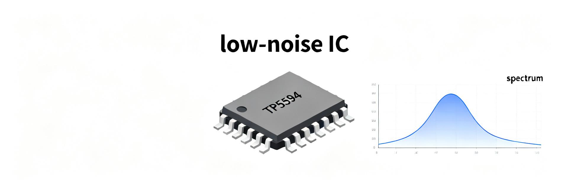
Measured noise density as low as 17 nV/√Hz at 1 kHz and a 0.1–10 Hz noise corner reported near 0.1 Hz make the TP5594-TR a strong candidate for ultra-low-noise front ends. This analysis translates datasheet specifications into actionable design guidance for precision measurement systems.
1 — Background & Where TP5594-TR Fits
The TP5594-TR targets sensor front-ends, precision integrators, and low-frequency measurement systems. Its zero-drift architecture suppresses offset and 1/f noise, improving long-term stability and reducing calibration overhead for DC to sub-Hz bandwidths.
1.1 — Target Applications and Architecture
Typical uses include weigh scales, precision thermometry, and bridge sensors. The chopper-stabilized design trades internal complexity for superior DC performance, ensuring minimal measurement wander in high-resolution ADC stages.
2 — Key Specs Overview
| Parameter | What to Check | Notes |
|---|---|---|
| Supply Range | Operating Headroom | Low-voltage optimization; check single-supply limits. |
| Input Offset | Typ / Max | Critical for DC error budget; check thermal settling. |
| Offset Drift | µV/°C | Use for worst-case temp error calculations. |
| Noise Density | 17 nV/√Hz @ 1kHz | Flat-band spectral noise floor. |
| 0.1–10 Hz Noise | Corner ~0.1 Hz | Indicates minimal 1/f contribution. |
3 — Noise & Drift Deep Dive
Integrating a 17 nV/√Hz flat spectrum from 0.1 Hz to 100 Hz yields RMS noise ≈ 17 · √(100 − 0.1) ≈ 170 nV RMS. Designers must account for the specific measurement bandwidth to convert spectral density into peak-to-peak voltage expectations.
4 — Measurement & Test Methods
Verification requires a battery-powered supply and guarded inputs to avoid thermal EMFs. Typical pitfalls include ground loops and thermocouple voltages at dissimilar metal junctions, which can easily swamp the sub-microvolt performance of the TP5594-TR.
5 — Design Recommendations
- Impedance Matching: Minimize source resistor values to reduce thermal noise (4kΩ ≈ 8 nV/√Hz).
- Layout: Use Kelvin sensing and solid ground planes to maintain signal integrity.
- Filtering: Implement an RC input filter sized for signal bandwidth to prevent aliasing and EMI.
Summary
The TP5594-TR offers a superior balance of low wideband noise and DC precision. Achieving datasheet performance requires disciplined layout, thermal management, and careful integration of the noise spectral density over the target bandwidth.
FAQ
What are the most critical TP5594-TR specs to check for a DC sensor amplifier?
Focus on input offset (typ/max), offset drift (µV/°C), and input bias current. These parameters define the static accuracy and the need for periodic system calibration.
How do I verify the TP5594-TR low-frequency noise in the lab?
Use a battery or ultra-low-noise LDO. Connect the amplifier in a high-gain configuration (e.g., Av=1000) with shielded inputs and use an FFT analyzer to capture the 0.1-10 Hz spectrum.
How should I budget for long-term drift when using TP5594-TR?
Calculate error as (Drift per °C × Temp Range) + (Long-term Drift Spec). For zero-drift parts, the temperature component is usually the dominant factor.
How does zero-drift architecture impact 1/f noise?
The internal chopping mechanism continuously corrects for DC offset, which effectively removes the 1/f (flicker) noise component, resulting in a flat noise floor down to very low frequencies.